
MCIMX6Y2DVM09AA
| Part Description |
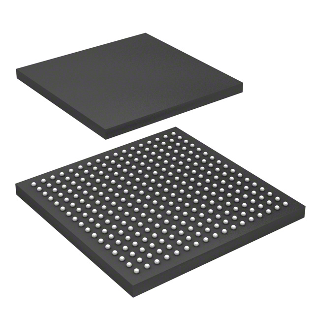
ARM® Cortex®-A7 Microprocessor IC i.MX6 1 Core, 32-Bit 900MHz 289-MAPBGA (14x14) |
|---|---|
| Quantity | 60 Available (as of October 8, 2026) |
| Product Category | Microprocessors |
|---|---|
| Part Series | i.MX 6Y |
| Manufacturer | NXP USA Inc. |
| Manufacturing Status | Active |
| Manufacturer Standard Lead Time | 16 Weeks |
| Datasheet |
Specifications & Environmental
| Co-Processors/DSP | Multimedia; NEON™ MPE | Core Processor | ARM® Cortex®-A7 | Device Package | 289-MAPBGA (14x14) | ||
|---|---|---|---|---|---|---|---|
| Display & Interface Controllers | Electrophoretic, LCD | ECCN | 5A992C | Ethernet | 10/100Mbps (2) | ||
| Graphics Acceleration | No | HTS Code | 8542.31.0001 | Moisture Sensitivity Level | 3 (168 Hours) | ||
| Mounting Method | Surface Mount | Mounting Type | Surface Mount | Number of Cores/Bus Width | 1 Core, 32-Bit | ||
| Operating Temperature | 0°C ~ 95°C (TJ) | Package / Case | 289-LFBGA | RAM Controllers | LPDDR2, DDR3, DDR3L | ||
| REACH Compliance | REACH Unaffected | RoHS Compliance | ROHS3 Compliant | Security Features | A-HAB, ARM TZ, CSU, SJC, SNVS | ||
| Speed | 900MHz | Supplier Device Package | 289-MAPBGA (14×14) | USB | USB 2.0 OTG + PHY (2) | ||
| Voltage – I/O | 1.8V, 2.8V, 3.3V |
Overview of MCIMX6Y2DVM09AA – IC MPU I.MX6 900MHz 289-MAPBGA
The MCIMX6Y2DVM09AA is a single-core ARM® Cortex®-A7 microprocessor IC from NXP Semiconductors' i.MX 6Y series. It delivers a 32-bit core running at up to 900 MHz and is specified for consumer and embedded applications.
Designed for compact, connected devices, this MPU combines CPU performance with integrated system-level features including multiple memory interfaces and a range of peripheral connectivity options to simplify board design and accelerate time to market.
Key Features
- Core & Performance Single ARM® Cortex®-A7 core, 32-bit, operating at up to 900 MHz for responsive application processing.
- Memory & Storage Interfaces Supports multiple memory controllers including LPDDR2, DDR3 and DDR3L, plus family-level support for NAND, NOR, eMMC and Quad SPI memory interfaces as described in the product documentation.
- Connectivity & I/O Dual 10/100 Mbps Ethernet ports, two USB 2.0 OTG + PHY interfaces, and CANbus support provide versatile wired connectivity for networking and peripheral integration.
- Display & Multimedia Includes display interface controllers suitable for electrophoretic and LCD panels, and multimedia/NEON™ MPE co-processor support for media processing acceleration.
- Security & System Protection On-chip security features listed for this part include A-HAB, ARM TrustZone (ARM TZ), CSU, SJC and SNVS for secure boot and runtime protection.
- Power & Integration Family documentation describes an integrated power management module to reduce external power-supply complexity and simplify power sequencing.
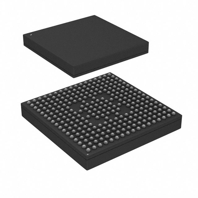
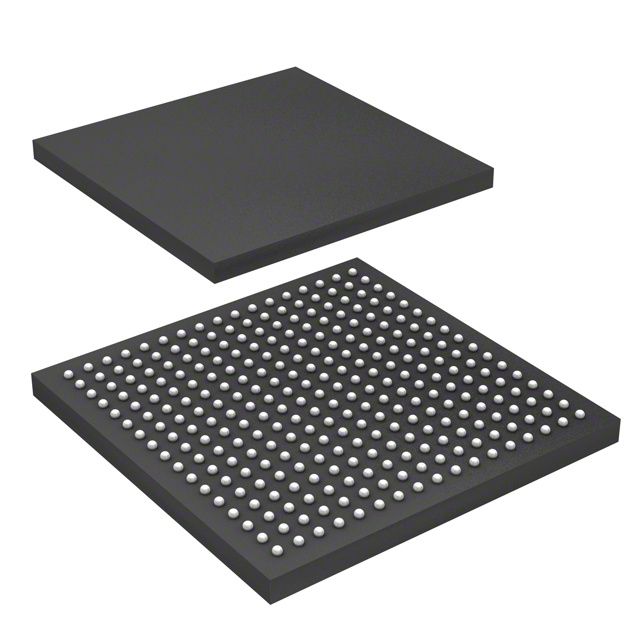
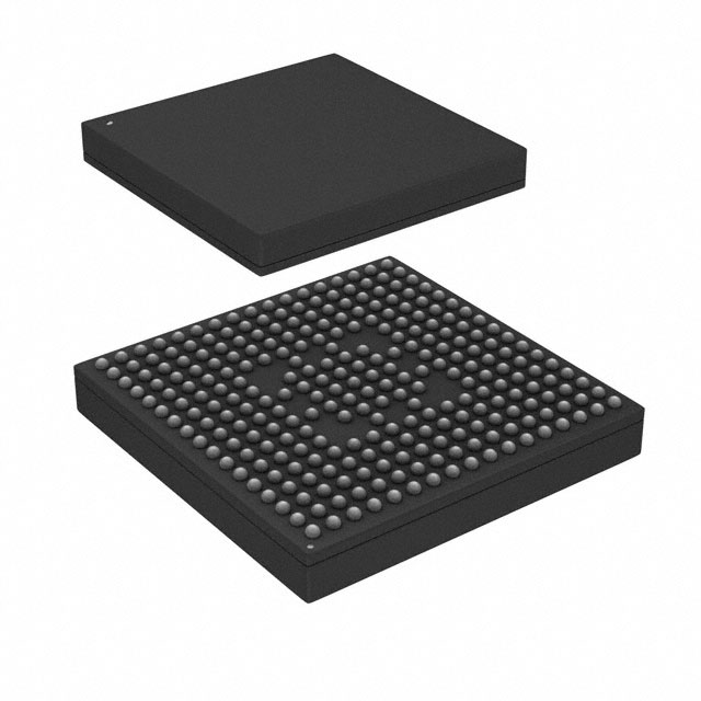
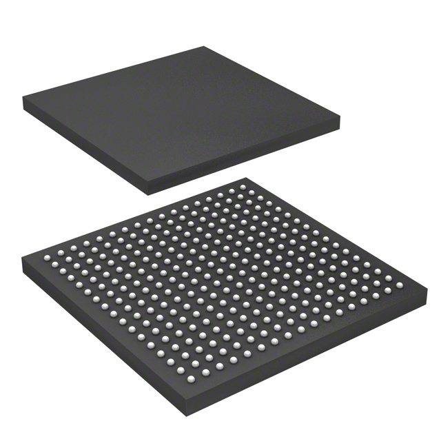
- Package & Mounting Supplied in a 289-ball MAPBGA package (14 mm × 14 mm), surface-mountable for compact system designs.
- Operating Range & Compliance Commercial operating temperature range of 0 °C to 95 °C and RoHS-compliant construction.
Typical Applications
- Connected Consumer Devices – Networked consumer electronics that require integrated Ethernet, USB OTG and multiple memory options to handle media and connectivity tasks.
- Embedded Displays & HMI – User interfaces and display controllers using the electrophoretic or LCD display interfaces supported by the device.
- IoT Gateways & Edge Devices – Edge nodes and gateway devices that leverage dual Ethernet, USB and CANbus for local connectivity and sensor aggregation.
- Multimedia-Enabled Embedded Systems – Compact systems that benefit from NEON™ MPE and multimedia co-processor support for media processing workloads.
Unique Advantages
- Single-core efficiency: A 900 MHz ARM Cortex-A7 core provides a balance of performance and power efficiency for embedded consumer applications.
- Flexible memory support: Multiple supported memory controllers (LPDDR2, DDR3, DDR3L) and family-level support for NAND/NOR/eMMC/Quad SPI simplify memory selection across use cases.
- Broad wired connectivity: Dual Ethernet ports, dual USB 2.0 OTG + PHY and CANbus deliver a wide set of I/O options for networking and peripheral integration.
- Integrated security features: Hardware security blocks including A-HAB and ARM TrustZone enhance platform security for secure boot and protected operation.
- Compact BGA footprint: The 289-MAPBGA (14×14 mm) package enables space-constrained system designs while maintaining a high pin count.
- Commercial-temperature qualification: Rated for 0 °C to 95 °C operation to meet typical consumer and embedded environmental requirements.
Why Choose MCIMX6Y2DVM09AA?
The MCIMX6Y2DVM09AA positions itself as a compact, integrated microprocessor for embedded and consumer-focused designs that require a capable 32-bit ARM Cortex-A7 core at 900 MHz. Its combination of flexible memory interfaces, multiple wired connectivity options and on-chip security features makes it suitable for connected devices, HMI and multimedia-enabled embedded applications.
For designers seeking a surface-mount MPU in a small MAPBGA package, the MCIMX6Y2DVM09AA offers an efficient, well-integrated starting point that reduces external component count and helps streamline board-level design.
Request a quote today to receive pricing and availability for the MCIMX6Y2DVM09AA and to discuss how this MPU can fit into your next embedded design.



















Date Founded: 2006
Headquarters: Eindhoven, North Brabant, Netherlands
Employees: 38,000+
Revenue: $10.53 Billion
Certifications and Memberships: ISO9001:2015, IATF16949:2016


