
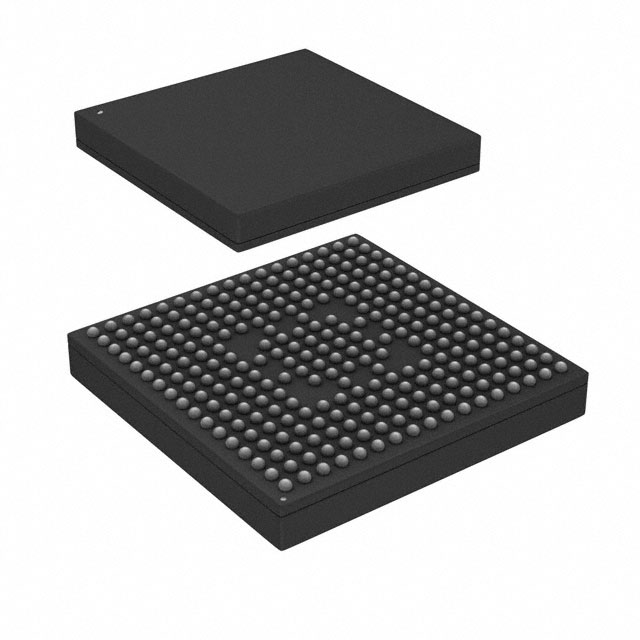
MCIMX6Y7DVK05AB
| Part Description |
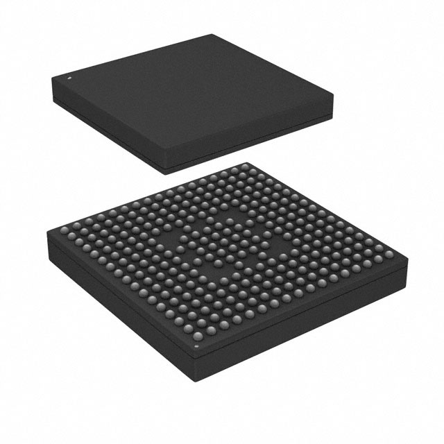
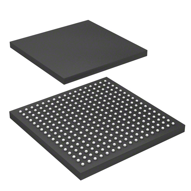
ARM® Cortex®-A7 Microprocessor IC i.MX6 1 Core, 32-Bit 528MHz 272-MAPBGA (9x9) |
|---|---|
| Quantity | 1,479 Available (as of October 8, 2026) |
| Product Category | Microprocessors |
|---|---|
| Part Series | i.MX 6Y |
| Manufacturer | NXP USA Inc. |
| Manufacturing Status | Active |
| Manufacturer Standard Lead Time | 16 Weeks |
| Datasheet |
Specifications & Environmental
| Co-Processors/DSP | Multimedia; NEON™ MPE | Core Processor | ARM® Cortex®-A7 | Device Package | 272-MAPBGA (9x9) | ||
|---|---|---|---|---|---|---|---|
| Display & Interface Controllers | Electrophoretic, LCD | ECCN | 5A992C | Ethernet | 10/100Mbps (2) | ||
| Graphics Acceleration | No | HTS Code | 8542.31.0001 | Moisture Sensitivity Level | 3 (168 Hours) | ||
| Mounting Method | Surface Mount | Mounting Type | Surface Mount | Number of Cores/Bus Width | 1 Core, 32-Bit | ||
| Operating Temperature | 0°C ~ 95°C (TJ) | Package / Case | 272-LFBGA | RAM Controllers | LPDDR2, DDR3, DDR3L | ||
| REACH Compliance | REACH Unaffected | RoHS Compliance | ROHS3 Compliant | Security Features | A-HAB, ARM TZ, CSU, SJC, SNVS | ||
| Speed | 528MHz | Supplier Device Package | 272-MAPBGA (9×9) | USB | USB 2.0 OTG + PHY (2) | ||
| Voltage – I/O | 1.8V, 2.8V, 3.3V |
Overview of MCIMX6Y7DVK05AB – IC MPU I.MX6 528MHz 272-MAPBGA
The MCIMX6Y7DVK05AB is a single-core ARM® Cortex®-A7 microprocessor IC from NXP Semiconductors, operating at 528 MHz in a compact 272-MAPBGA (9×9 mm) package. Designed for embedded and consumer applications, it combines a 32-bit processing core with multimedia coprocessor support and a range of integrated peripheral interfaces.
This device is positioned for connected consumer and embedded designs that require efficient application processing, flexible memory options, and integrated connectivity while maintaining a consumer qualification level and RoHS compliance.
Key Features
- Core Single ARM® Cortex®-A7 32-bit core running at 528 MHz for application processing.
- Coprocessors Multimedia and NEON™ MPE support for accelerated media and signal processing tasks.
- Memory Interfaces Compatible with LPDDR2, DDR3 and DDR3L memory controllers to suit a range of performance and power targets.
- Connectivity Dual 10/100 Mbps Ethernet interfaces and dual USB 2.0 OTG with PHY for networked and peripheral connections.
- Display and I/O Display interface controllers for electrophoretic and LCD panels plus additional interfaces including CAN for vehicle or industrial networks.
- Security Integrated security features include A-HAB, ARM TrustZone (ARM TZ), CSU, SJC and SNVS to support secure boot and runtime security functions.
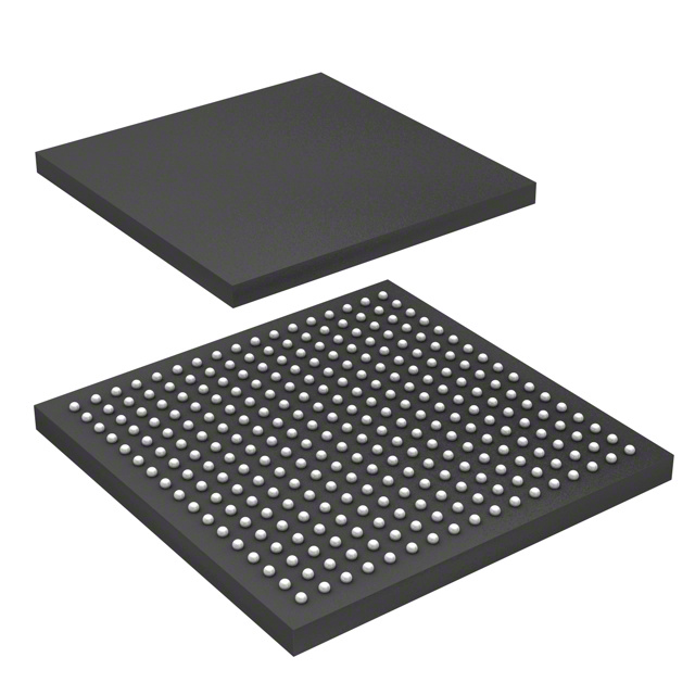
- Package & Mounting Supplied in a 272-MAPBGA (9×9 mm) surface-mount package; package case listed as 272-LFBGA.
- Qualification & Compliance Consumer qualification and RoHS compliance for environmentally conscious design requirements.
- Operating Range Rated for an operating temperature range of 0 °C to 95 °C.
Typical Applications
- Connected Consumer Devices — Application processing and peripheral integration for consumer-focused connected products.
- Human-Machine Interfaces & Displays — Drive electrophoretic or LCD displays and manage UI tasks with the onboard display controllers.
- Networked Embedded Systems — Dual Ethernet and CAN support enable use in sensor gateways, controllers, and networked appliances.
- USB-enabled Peripherals — USB 2.0 OTG with integrated PHY for attaching or hosting USB devices.
Unique Advantages
- Compact MAPBGA footprint: 272-MAPBGA (9×9 mm) packaging reduces PCB area while supporting surface-mount assembly.
- Broad memory flexibility: Support for LPDDR2, DDR3 and DDR3L lets designers choose memory technologies to match performance and power budgets.
- Integrated connectivity: Built-in Ethernet, USB OTG and CAN interfaces reduce external component count and simplify system design.
- Security-ready platform: On-chip security features (A-HAB, ARM TZ, CSU, SJC, SNVS) enable secure boot and trusted execution capabilities.
- Designed for consumer applications: Consumer qualification and RoHS compliance align the part with mainstream embedded product requirements.
- Documented by manufacturer: Product is supported by NXP Semiconductors documentation and technical data to aid system integration.
Why Choose MCIMX6Y7DVK05AB?
The MCIMX6Y7DVK05AB delivers a balanced single-core ARM® Cortex®-A7 processing solution for embedded and consumer designs that demand integrated connectivity, memory flexibility and built-in security. Its 528 MHz core, multimedia coprocessor support, and multiple I/O options make it suitable for display-driven interfaces, networked devices and USB-enabled peripherals.
Backed by NXP Semiconductors' product documentation and supplied in a compact 272-MAPBGA package with a consumer-grade operating range, this microprocessor is a practical choice for designers seeking a documented, RoHS-compliant building block for connected embedded applications.
Request a quote today to discuss pricing and availability for MCIMX6Y7DVK05AB and to receive technical documentation for integration into your design.



















Date Founded: 2006
Headquarters: Eindhoven, North Brabant, Netherlands
Employees: 38,000+
Revenue: $10.53 Billion
Certifications and Memberships: ISO9001:2015, IATF16949:2016


