
MIMX8UX5FVLFZAC
| Part Description |
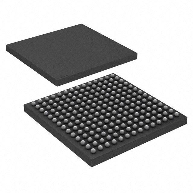
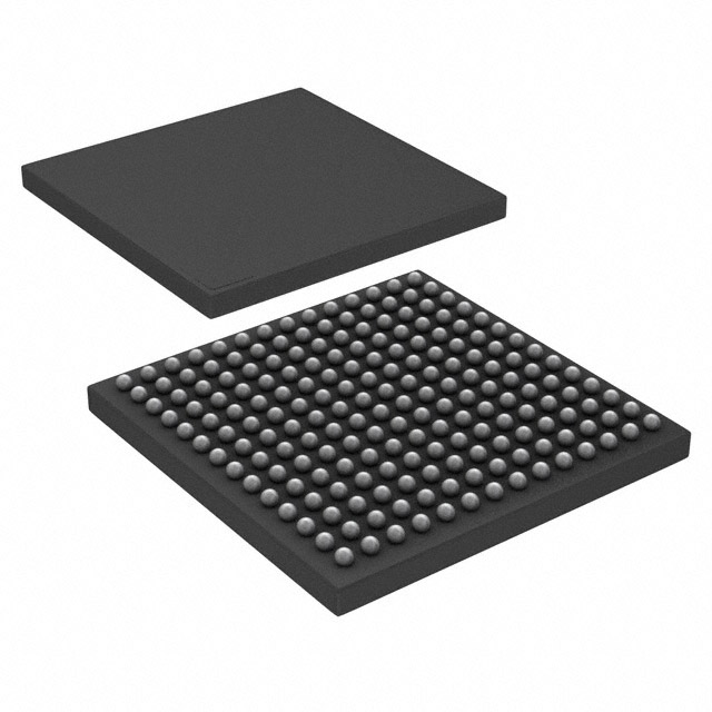
ARM® Cortex®-A53, ARM® Cortex®-M4F Microprocessor IC i.MX8Q 3 Core, 64-Bit 1.2GHz, 264MHz 609-FBGA (21x21) |
|---|---|
| Quantity | 1,121 Available (as of October 8, 2026) |

| Product Category | Microprocessors |
|---|---|
| Part Series | i.MX 8UX |
| Manufacturer | NXP USA Inc. |
| Manufacturing Status | Active |
| Manufacturer Standard Lead Time | 32 Weeks |
| Datasheet |
Specifications & Environmental
| Co-Processors/DSP | Multimedia; NEON, Hi-Fi4 DSP | Core Processor | ARM® Cortex®-A53, ARM® Cortex®-M4F | Device Package | 609-FBGA (21x21) | ||
|---|---|---|---|---|---|---|---|
| Display & Interface Controllers | LCD, LVDS, MIPI-CSI, MIPI-DSI | ECCN | N/A | Ethernet | 10/100/1000Mbps (2) | ||
| Graphics Acceleration | Yes | HTS Code | N/A | Moisture Sensitivity Level | N/A | ||
| Mounting Method | Surface Mount | Mounting Type | Surface Mount | Number of Cores/Bus Width | 3 Core, 64-Bit | ||
| Operating Temperature | – | Package / Case | 609-BFBGA | RAM Controllers | DDR3L SDRAM, LPDDR4 DRAM | ||
| REACH Compliance | REACH Unaffected | RoHS Compliance | ROHS3 Compliant | Security Features | 3DES, A-HAB, ARM TZ, CAAM, DES, MD5, SHA, SNVS | ||
| Speed | 1.2GHz, 264MHz | Supplier Device Package | 609-FBGA (21×21) | USB | USB 2.0 OTG + PHY (1), USB 3.0 OTG + PHY (1) | ||
| Voltage – I/O | 1.8V, 2.5V, 3.3V |
Overview of MIMX8UX5FVLFZAC – I.MX8 QXP 21X21
The MIMX8UX5FVLFZAC is an NXP Semiconductors microprocessor IC featuring ARM® Cortex®-A53 and ARM® Cortex®-M4F cores in a 3-core, 64-bit configuration. With a primary application-core frequency of 1.2 GHz and a companion core at 264 MHz, this device targets embedded designs that require application-class processing alongside integrated peripheral support.
Engineered for multimedia and connected embedded systems, the device combines general-purpose compute, DSP acceleration and comprehensive I/O to address HMI, imaging, secure connectivity and industrial control segments while providing a highly integrated package option for compact designs.
Key Features
- Core Architecture ARM® Cortex®-A53 plus ARM® Cortex®-M4F; 3 cores, 64-bit compute backbone with a 1.2 GHz application core and a 264 MHz companion core.
- DSP and Multimedia Acceleration Integrated multimedia co-processors including NEON and Hi-Fi4 DSP support and graphics acceleration for advanced audio and processing tasks.
- Memory Interfaces On-chip controllers for DDR3L SDRAM and LPDDR4 DRAM provide flexible external memory choices for performance and capacity scaling.
- Display and Imaging Display interface controllers for LCD and LVDS plus MIPI-CSI and MIPI-DSI for camera and panel connectivity.
- Connectivity Dual Gigabit Ethernet (10/100/1000 Mbps), USB 2.0 OTG with PHY (1) and USB 3.0 OTG with PHY (1), plus CANbus support for robust wired connectivity.
- Security Hardware and software security features including A-HAB, ARM TrustZone (ARM TZ), CAAM, 3DES, DES, MD5, SHA and SNVS for secure boot and cryptographic operations.
- Package and Mounting 609-FBGA package (21 mm × 21 mm) designed for surface-mount assembly to support compact board layouts.
- Compliance RoHS compliant.
Typical Applications
- Human–Machine Interfaces (HMI) Drive displays and multimedia UI layers using the integrated display controllers and graphics acceleration.
- Imaging and Vision Camera and sensor interfacing via MIPI-CSI and on-chip processing resources for image handling and preprocessing.
- Secure Connected Devices Gateways and edge devices leveraging dual Gigabit Ethernet, USB 3.0, and onboard security features for encrypted communications and secure boot.
- Industrial Control and Automation Embedded control nodes using CANbus and mixed I/O to interface with sensors, actuators and field networks.
Unique Advantages
- Balanced Heterogeneous Processing Combination of Cortex‑A53 and Cortex‑M4F cores provides both application-level compute and companion processing capability in a single device.
- Integrated Multimedia and DSP Engines NEON and Hi‑Fi4 DSP support with graphics acceleration reduces external processor dependency for audio, vision and signal tasks.
- Comprehensive Connectivity Suite Dual Gigabit Ethernet, USB 2.0/3.0 OTG with PHY and CANbus simplify system integration and reduce BOM complexity.
- Hardware Security Building Blocks A-HAB, ARM TrustZone and CAAM among other cryptographic primitives enable secure boot, encryption and authenticated workflows.
- Flexible Memory Support DDR3L and LPDDR4 memory controller support allows designers to select memory technology that matches performance and power targets.
- Compact, Production-Ready Package 609‑FBGA (21×21 mm) surface‑mount package streamlines board real estate for compact embedded platforms.
Why Choose MIMX8UX5FVLFZAC?
The MIMX8UX5FVLFZAC positions itself as a versatile embedded microprocessor combining multi‑core compute, DSP acceleration and a broad set of integrated I/O and security features. It is well suited to designers building connected multimedia devices, secure edge appliances and industrial control systems that benefit from on-chip connectivity and cryptographic capabilities.
Backed by NXP Semiconductors’ product family and technical documentation, this device offers a compact 609‑FBGA footprint and feature set intended to simplify system design while providing scalable memory and interface options for production deployments.
Request a quote or submit your requirements today to check availability and pricing for the MIMX8UX5FVLFZAC.




















Date Founded: 2006
Headquarters: Eindhoven, North Brabant, Netherlands
Employees: 38,000+
Revenue: $10.53 Billion
Certifications and Memberships: ISO9001:2015, IATF16949:2016


