
S32G398AACK1VUCR
| Part Description |
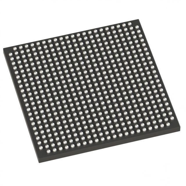
ARM® Cortex®-A53, ARM® Cortex®-M7 Microprocessor IC S32G3 3 Core, 64-Bit/8 Core, 32-Bit 400MHz, 1.3GHz 525-FCPBGA (19x19) |
|---|---|
| Quantity | 283 Available (as of October 8, 2026) |

| Product Category | Microprocessors |
|---|---|
| Part Series | S32G398 |
| Manufacturer | NXP USA Inc. |
| Manufacturing Status | Active |
| Manufacturer Standard Lead Time | 26 Weeks |
| Datasheet |
Specifications & Environmental
| Co-Processors/DSP | Multimedia; NEON | Core Processor | ARM® Cortex®-A53, ARM® Cortex®-M7 | Device Package | 525-FCPBGA (19x19) | ||
|---|---|---|---|---|---|---|---|
| ECCN | N/A | Ethernet | 2.5Gbps (3) | Graphics Acceleration | No | ||
| HTS Code | N/A | Moisture Sensitivity Level | N/A | Mounting Method | Surface Mount | ||
| Mounting Type | Surface Mount | Number of Cores/Bus Width | 3 Core, 64-Bit/8 Core, 32-Bit | Operating Temperature | -40°C ~ 105°C (TA) | ||
| Package / Case | 525-FBGA, FCBGA | RAM Controllers | DDR3L SDRAM, LPDDR4 DRAM | REACH Compliance | REACH Unaffected | ||
| RoHS Compliance | ROHS3 Compliant | Security Features | ARM TZ, Cryptography, Random Number Generator, Secure Fusebox, Secure Memory, XRDC | Speed | 400MHz, 1.3GHz | ||
| Supplier Device Package | 525-FCPBGA (19×19) | USB | USB 2.0 OTG (1) | Voltage – I/O | 1.8V, 3.3V |
Overview of S32G398AACK1VUCR – 8× ARM® Cortex®‑A53 1.3GHz, 3× ARM® Cortex®‑M7 400MHz Multi-Core Microprocessor
The S32G398AACK1VUCR is a multi-core microprocessor IC from NXP Semiconductors, combining ARM® Cortex®‑A53 and ARM® Cortex®‑M7 cores in a compact 525‑FCPBGA (19×19) package. The device integrates high-performance application cores alongside real-time microcontroller cores to address embedded processing needs.
Designed for embedded and industrial applications, the part delivers a mix of compute performance, deterministic control, networking interfaces and on-chip security primitives to simplify system integration and meet industrial temperature requirements.
Key Features
- Core Architecture & Performance Dual-core families: ARM® Cortex®‑A53 and ARM® Cortex®‑M7. Core configuration indicated as 8× A53 at 1.3 GHz and 3× M7 at 400 MHz for task-parallel and real-time workloads.
- Memory Interfaces Integrated controllers for DDR3L SDRAM and LPDDR4 DRAM to support high-bandwidth application and system memory requirements.
- Networking & Connectivity Three 2.5Gbps Ethernet interfaces provide high-speed wired networking; includes a single USB 2.0 OTG port and CANbus support for common embedded communication needs.
- Security Features On-chip security primitives including ARM TrustZone, cryptography engines, a random number generator, secure fusebox, secure memory and XRDC for hardware-enforced isolation and secure boot/building blocks.
- Multimedia Acceleration DSP/NEON multimedia coprocessor support for accelerated signal and media processing workloads.
- Package & Mounting 525‑FCPBGA (19×19) surface-mount package (525‑FBGA/FCBGA family) suitable for compact embedded board designs.
- Operating Range & Qualification Industrial qualification with an operating temperature range of −40°C to 105°C and RoHS compliance for broad environmental compatibility.
Typical Applications
- Industrial Networking & Control Use the multi‑gigabit Ethernet interfaces and CANbus to implement high-throughput industrial communication nodes and real-time controllers.
- Secure Embedded Gateways Combine ARM® Cortex®‑A53 application processing with on-chip security features to implement secure edge routing and protocol translation.
- Real-Time Control Systems Leverage ARM® Cortex®‑M7 cores for deterministic control tasks alongside A53 cores for higher-level processing in embedded control platforms.
- High-Bandwidth Embedded Compute Support memory-intensive and multimedia workloads using DDR3L/LPDDR4 interfaces and NEON/DSP acceleration.
Unique Advantages
- Heterogeneous Multi-Core Integration: Combines high-performance Cortex‑A53 application cores with Cortex‑M7 real-time cores for consolidated system design and task partitioning.
- Built-in Industrial Connectivity: Multiple 2.5Gbps Ethernet ports plus CANbus and USB OTG reduce the need for external networking controllers and simplify BOM.
- Comprehensive On-Chip Security: Hardware security primitives including TrustZone, cryptography, RNG and secure fusebox enable stronger system-level protection and secure provisioning.
- Memory Flexibility: Support for DDR3L and LPDDR4 memory technologies allows designers to optimize for cost or bandwidth as required.
- Designed for Industrial Environments: Industrial qualification and −40°C to 105°C operating range provide robustness for embedded deployments.
- Compact Surface-Mount Package: 525‑FCPBGA (19×19) packaging supports dense PCB layouts while offering necessary I/O for embedded systems.
Why Choose S32G398AACK1VUCR?
The S32G398AACK1VUCR positions itself as a flexible, integrated microprocessor option for embedded and industrial designs that require a combination of application-level processing, real-time control and secure connectivity. Its heterogeneous mix of ARM® Cortex®‑A53 and Cortex®‑M7 cores, along with multiple 2.5Gbps Ethernet interfaces, CANbus, and on-chip security primitives, streamlines system architecture and reduces external component count.
Engineers targeting industrial networking, secure edge processing or high-bandwidth embedded compute will find the device’s industrial temperature qualification, compact FCPBGA package and memory interface options suited to demanding deployments where performance and integration matter.
Request a quote or contact sales to discuss availability and pricing for S32G398AACK1VUCR and to submit a sourcing inquiry today.




















Date Founded: 2006
Headquarters: Eindhoven, North Brabant, Netherlands
Employees: 38,000+
Revenue: $10.53 Billion
Certifications and Memberships: ISO9001:2015, IATF16949:2016


