
SPC5643LFF2MMM1
| Part Description |
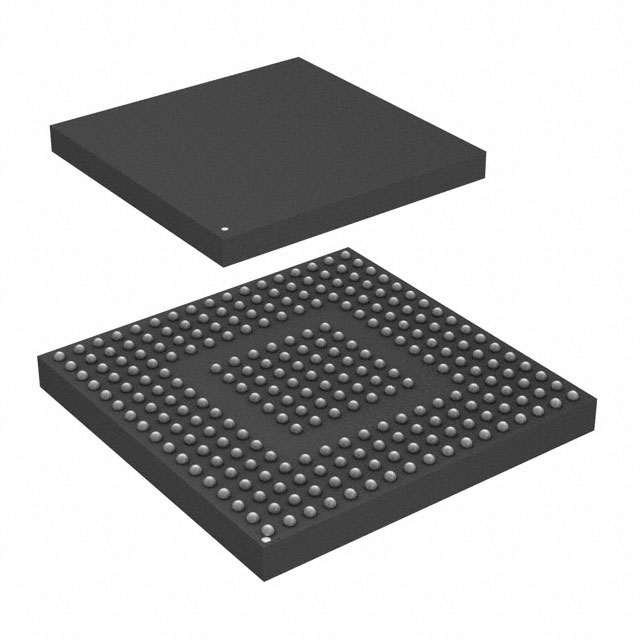
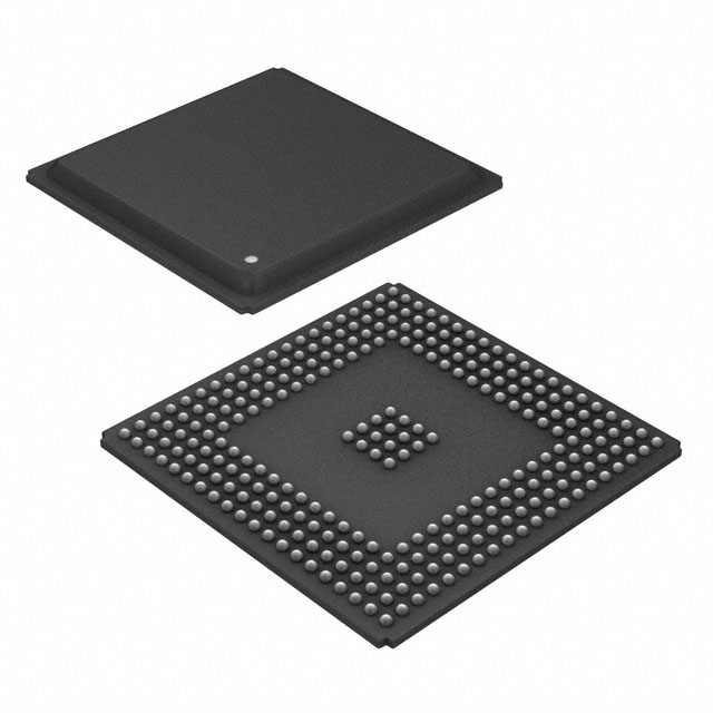
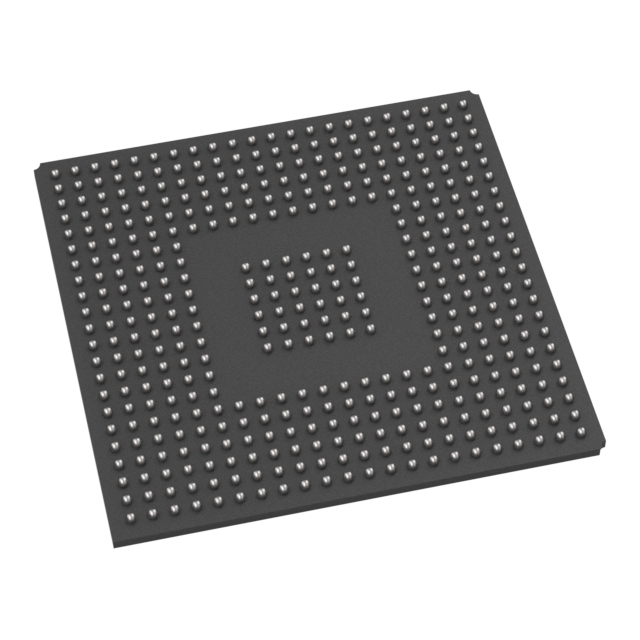
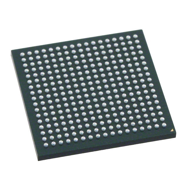
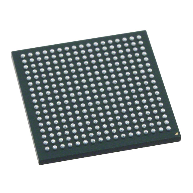
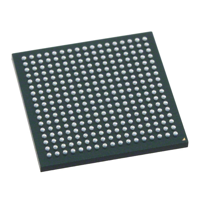
e200z4 MPC56xx Qorivva Microcontroller IC 32-Bit Dual-Core 120MHz 1MB (1M x 8) FLASH 257-LFBGA (14x14) |
|---|---|
| Quantity | 440 Available (as of October 8, 2026) |
| Product Category | Microprocessors |
|---|---|
| Part Series | SPC5643 |
| Manufacturer | NXP USA Inc. |
| Manufacturing Status | Active |
| Manufacturer Standard Lead Time | 16 Weeks |
| Datasheet |
Specifications & Environmental
| Connectivity | CANbus, FlexRay, LINbus, SPI, UART/USART | Core Processor | e200z4 | Core Size | 32-Bit Dual-Core | ||
|---|---|---|---|---|---|---|---|
| Data Converters | A/D 32x12b | Device Package | 257-LFBGA (14x14) | ECCN | 3A991A2 | ||
| Grade | Automotive | HTS Code | 8542.31.0001 | Moisture Sensitivity Level | 3 (168 Hours) | ||
| Mounting Method | Surface Mount | Mounting Type | Surface Mount | Operating Temperature | -40°C ~ 125°C (TA) | ||
| Oscillator Type | Internal | Package / Case | 257-LFBGA | Peripherals | DMA, POR, PWM, WDT | ||
| Program Memory Size | 1MB (1M x 8) | Program Memory Type | FLASH | RAM Size | 128K x 8 | ||
| REACH Compliance | REACH Unaffected | RoHS Compliance | ROHS3 Compliant | Speed | 120MHz | ||
| Supplier Device Package | 257-LFBGA (14×14) | Voltage – Supply (Vcc/Vdd) | 3V ~ 5.5V |
Overview of SPC5643LFF2MMM1 – 32‑Bit Dual‑Core MCU, 1 MB Flash
The SPC5643LFF2MMM1 from NXP Semiconductors is a 32‑bit dual‑core microcontroller based on e200z4 cores with 1 MB of on‑chip FLASH. With 120 MHz core speed, 3.3 V I/O and an integrated ADC interface, it is intended for embedded and industrial applications that require balanced processing capability, integrated analog I/O and extended temperature operation.
Packaged in a compact 257‑LFBGA (14×14) surface‑mount package and qualified for industrial use, the device targets applications that need on‑board code storage, multiple processing contexts and reliable operation across a wide temperature range.
Key Features
- Core – Dual e200z4 32‑bit cores at 120 MHz providing parallel processing capability for multi‑task and control-oriented workloads.
- Memory – 1 MB (1M × 8) on‑chip FLASH for application code and data storage.
- Power and I/O – 3.3 V I/O signaling for common embedded interface compatibility.
- Analog and Interfaces – Integrated ADC interface to support sensor acquisition and analog signal measurement.
- Package and Mounting – 257‑LFBGA (14×14) supplier device package, surface mount for compact PCB integration.
- Operating Range and Qualification – Industrial qualification with an operating temperature range of −40 °C to 125 °C for extended environmental tolerance.
- Regulatory Status – RoHS compliant.
- Graphics Acceleration – No graphics acceleration included.
Typical Applications
- Industrial Control – Use the dual cores and ADC interface for control algorithms, sensor acquisition and deterministic task separation in factory automation and process control.
- Motor and Drive Systems – On‑chip FLASH and dual processing capability support control firmware and real‑time loop handling for motor control applications.
- Instrumentation – Extended temperature range and ADC integration make this device suitable for instrumentation and measurement systems operating in harsh environments.
- Embedded Systems – Compact LFBGA package and 3.3 V I/O enable integration into space‑constrained embedded platforms requiring local application storage and processing.
Unique Advantages
- Dual‑core processing: Enables separation of high‑priority control tasks and background processing to improve system determinism.
- 1 MB on‑chip FLASH: Provides ample code and data space for complex embedded applications without immediate external memory requirements.
- Wide operating temperature: −40 °C to 125 °C supports deployments in demanding thermal environments.
- Integrated ADC interface: Simplifies sensor interfacing and reduces bill‑of‑materials by handling analog inputs on‑chip.
- Compact LFBGA package: 257‑ball 14×14 LFBGA delivers high integration density for space‑sensitive PCB layouts.
- Industrial qualification and RoHS compliance: Aligns with environmental and industrial usage requirements.
Why Choose SPC5643LFF2MMM1?
The SPC5643LFF2MMM1 combines dual e200z4 32‑bit cores at 120 MHz with 1 MB of on‑chip FLASH, integrated ADC capability and a compact 257‑LFBGA package to deliver a well‑rounded solution for embedded and industrial designs. Its 3.3 V I/O and industrial temperature rating support reliable integration into a wide range of systems that require local code storage and analog interfacing.
Backed by NXP Semiconductors and qualified for industrial use, this device is suited for engineers looking for a scalable processing platform with on‑board memory and analog capability, supporting long‑term deployments in challenging environmental conditions.
Request a quote or submit a pricing and availability inquiry for SPC5643LFF2MMM1 to get started with your design procurement.





















Date Founded: 2006
Headquarters: Eindhoven, North Brabant, Netherlands
Employees: 38,000+
Revenue: $10.53 Billion
Certifications and Memberships: ISO9001:2015, IATF16949:2016


