Suntsu PCB Antennas

Suntsu PCB Antennas

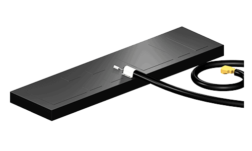
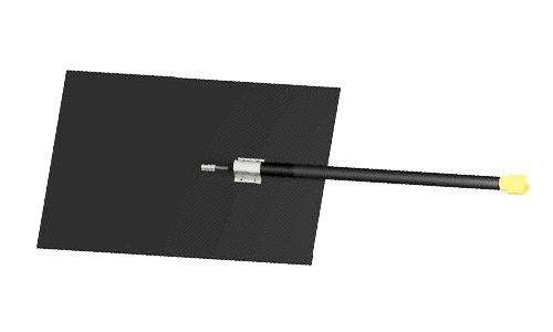
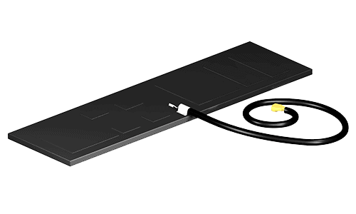
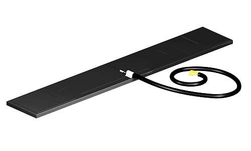
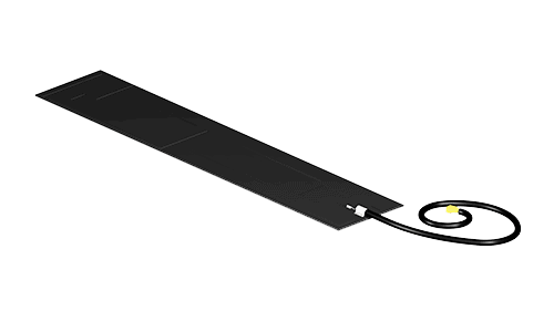
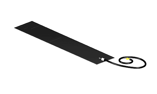
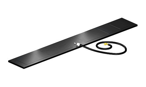
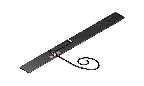
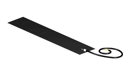
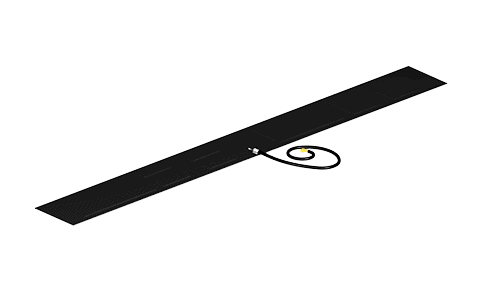
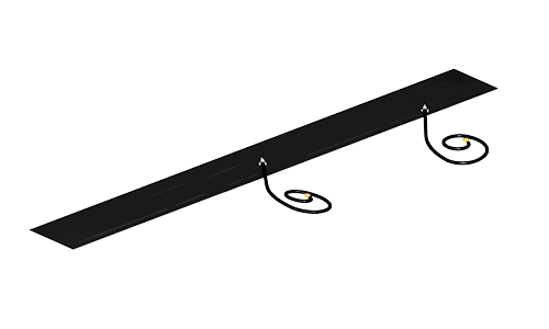
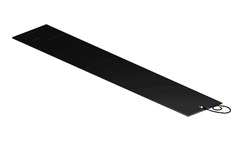
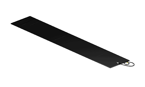
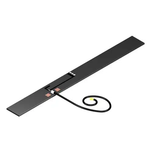
Suntsu PCB Antennas offer WiFi, ISM and Mobile communications serving the Smart grid, IOT, Enterprise, Automotive, Telecommunications and Consumer Wireless Industries. We offer a wide range of Frequency bands, including but not limited to, WiFi/ZigBee/Bluetooth band (2400-2500MHz), WiFi Dual band (2400-2500MHz & 4900-5900MHz), ISM bands (433MHz, 863-870MHz & 902-928MHz) and 3G/GSM/LTE full band (824-960MHz, 1710-2170MHz, 2300-2400MHz & 2490-2690MHz). With package sizes from 17.0×4.5mm up to 75.0×8.5mm. Pick out a standard part number from the data sheets listed below or contact us to request any custom parameters or physical modifications that you may desire and we will design to your specific needs.

Suntsu Part NumberImagesPackage (mm)Frequency Band (MHz)ApplicationApplicationDatasheet
SATPC-17A4FJ-WFB5SATPC-17A4FJ-WFB517.0 x 4.5 x 0.95150-5900WiFiWiFi 5GHzDatasheet Download
SATPC-24A33AC5-UWB2SATPC-17A4FJ-WFB524.0 x 33.0 x 0.256250 – 8250UWBUltra WidebandDatasheet Download
SATPC-25A7AF-WFB2SATPC-25A7AF-WFB225.0 x 7.0 x 0.52400-2500 & 4900-5900WiFiWiFi Dual bandDatasheet Download
SATPC-30A5AF-WFB1SATPC-30A5AF-WFB130.0 x 5.0 x 0.52400-2500WiFiWiFi/Zigbee/BluetoothDatasheet Download
SATPC-35A7AF-ISB5SATPC-62A7AB5-ISB135.0 x 7.0 x 0.5863-870ISMISM 433MHzDatasheet Download
SATPC-35A7AB5-ISB5SATPC-35A7AB5-ISB535.0 x 7.0 x 0.15863-870ISMISM 433MHzDatasheet Download
SATPC-35A7AF-ISB7SATPC-35A7AF-ISB735.0 x 7.0 x 0.5902-928ISMISM 433MHzDatasheet Download
SATPC-35A7AB5-ISB7SATPC-35A7AB5-ISB5-135.0 x 7.0 x 0.15902-928ISMISM 433MHzDatasheet Download
SATPC-35A7AF-CEB4SATPC-35A7AF-CEB435.0 x 7.0 x 0.5824-960 & 1710-21703G/GSM/LTE3G/GSMDatasheet Download
SATPC-35A7AB5-CEB4SATPC-35A7AB5-CEB4.png35.0 x 7.0 x 0.15824-960 & 1710-21703G/GSM/LTE3G/GSMDatasheet Download
SATPC-40A6AF-WFB2SATPC-40A6AF-WFB2-140.0 x 6.0 x 0.52400-2500 & 4900-5900WiFiWiFi Dual bandDatasheet Download
SATPC-50F5AF-WFB1SATPC-50F5AF-WFB150.5 x 5.0 x 0.52400-2500WiFiWiFi/Zigbee/BluetoothDatasheet Download
SATPC-62A7AF-ISB1SATPC-62A7AF-ISB162.0 x 7.0 x 0.5433ISMISM 433MHzDatasheet Download
SATPC-62A7AB5-ISB1SATPC-62A7AB5-ISB162.0 x 7.0 x 0.15433ISMISM 433MHzDatasheet Download
SATPC-75A8FF-CEB4SATPC-75A8FF-CEB475.0 x 8.5 x 0.5824-960 & 1710-21703G/GSM/LTE3G/GSMDatasheet Download
SATPC-75A8FB5-CEB4SATPC-75A8FB5-CEB475.0 x 8.5 x 0.15824-960 & 1710-21703G/GSM/LTE3G/GSMDatasheet Download
SATPC-75A8FF-CEB5SATPC-75A8FF-CEB575.0 x 8.5 x 0.5824-960, 1710-2170& 2400-25003G/GSM/LTE3G/GSM + WiFi(2.4GHz)Datasheet Download
SATPC-75A8FF-CEB2SATPC-75A8FF-CEB275.0 x 8.5 x 0.5824-960, 1710-2170, 2300-2400 & 2490-26903G/GSM/LTE3G/GSM/LTE full bandDatasheet Download
SATPC-120A13AF-CEB2SATPC-120A13AF-CEB2120.0 x 13.0 x 0.5824-960, 1710-2170, 2300-2400 & 2490-26903G/GSM/LTE3G/GSM/LTE full bandDatasheet Download
SATPC-111A20AI-CEB10SATPC-111A20AI-CEB10111.0 x 20.0 x 0.8698-960, 1427.9-1510.9, 1559-1610, 1695-2200, 2300-2700, 3400-3600LTELTE full bandDatasheet Download

What is a PCB Antenna?

An antenna printed directly on the printed circuit board material (PCB) is a PCB antenna. Our PCB antenna is a separate component printed onto FR4 or rigid-flex PCB that connects with a cable to the main circuit board. This approach avoids many of the significant disadvantages of printing an antenna directly as a trace PCB antenna on the circuit board. It allows you to modify the circuit board without changing the antenna if you upgrade your design.

PCB Antenna Applications

The development of small-scale printed circuit boards and wireless communication increases the innovative uses for PCB antennas. Some of the applications include:

  • Communication – devices, and people communicate using radio waves with receiving and transmitting antenna instead of electric cable.
  • IoT – more of our household appliances have acquired PCB antenna so they can make your life a little easier in surprising and entertaining ways.
  • Medical – medical science adapts to take advantage of new technology, and current innovations are coming from wireless communication for treatment, diagnoses, and monitoring.
  • Automotive – driverless cars are coming, but there are more modest applications like collision warning and assisted parking.
  • Robots – for fun activities or practical, control your vacuum cleaner or lawnmower through WiFi, and where you use WiFi, you have antennas.

Advantages and Disadvantages of a PCB Antenna

The main advantages include:

  • Versatile – you can design your ideal antenna and integrate it with your application.
  • Small scale and low profile – you can mount on any flat surface.
  • Optimal design – gives a high gain with excellent, reliable performance,

The downsides are:

  • A PCB antenna needs to be installed considering EMI related products like wireless modules, battery, metals.
  • These antennas need a stable environment for optimum operation and are susceptible to noise. For example, you need an unreasonably large antenna.

What type of frequency bands do we offer?

We offer a wide range of Frequency bands, including but not limited to,

  • WiFi/ZigBee/Bluetooth band (2.4-2.5GHz)
  • WiFi Dual-band (2.4-2.5GHz and 4.9-5.9GHz)
  • ISM bands (433MHz, 863-870MHz & 902-928MHz)
  • 3G/GSM/LTE full band (699-960MHz, 1710-2170MHz, 2300-2400MHz and 2490-2690MHz).

How an electromagnetic wave works depends on its frequency. There is a broad spectrum of electromagnetic waves with various potential uses. The most useful for communication purposes fall in the radio and microwave frequencies. The radio frequency band stretches from 30Hz to 300GHz, and our PCB antenna work in the radio frequency range. Our standard components include Bluetooth antenna PCB and WiFi antenna PCB.

The International Telecommunications Union regulates the use of radio bands for different applications. You pick the frequency of the PCB antenna to match your application.

A GPS PCB antenna works in the GPS frequency range of 1.5 GHz, and that would be a custom order from us, or you can opt for a GPS patch antenna. A 13.56MHz PCB antenna uses the RFID and NFC tag frequencies, and we can create a custom PCB antenna for this application, but we offer a broad range of NFC antennas.

Want to design your own?

A custom PCB antenna can significantly lower your manufacturing costs because you create an antenna to match your application design rather than compromising on the other design and cost elements to use a non-ideal antenna.

The critical elements of PCB antenna design are:

  • Antenna length – alters the operation frequency.
  • Feed – how you power the antenna makes a difference to the radiation pattern.
  • Groundplane – shape and size affect performance and efficiency.
  • Type – simple loop or more complex shape and layers.
  • Operating environment inside the enclosure.
  • Materials – dielectric of PCB board and the RF properties of other components.

It is not helpful to design a PCB antenna in isolation because it must work with the enclosure and other components. Our professional team has plenty of experience designing PCB antennas for various applications and can recommend designs and alternatives for your application.

Frequently Asked Questions

Our PCB antennas and chip antennas are separate components that you add to your circuit board inside the device enclosure, but the chip antenna occupies less space.  The PCB antenna is larger than the chip antenna, and typically larger antennas are more efficient. Still, the PCB antenna requires plenty of space around it and separation from the other components and metal objects. Correctly implemented, a PCB antenna performs better than the equivalent chip antenna. 

For a PCB antenna to have maximum effectiveness, the design and fabrication aim at minimizing passive intermodulation (PIM) in the circuit materials. PIM is the creation of unwanted harmonic signals or interference with the desired signal transmission and reception. Inhomogeneous materials in circuit joints, rough copper in the conductive layer, corrosion, and plating materials can adversely impact PIM levels.  The substrate's dielectric coefficient influences performance but not as much as a rough copper trace compared with a smooth one. For optimum PCB antenna performance, you want smooth copper in the PCB antenna design. Immersion tin plating gives better performance than ferromagnetic materials containing nickel. Plus, covering clean copper circuits with a protective layer of solder mask gives better PIM levels than leaving the circuits bare. Finally, a clean etching process avoiding copper dendrites along the circuit edges reduces the prospect of unwanted PIM. 

Designing PCB antenna and other wireless systems involve compromises: 

  • A high data rate means a shorter distance between the antenna for effective operation. 
  • A large PCB antenna has a longer range but occupies more physical space on enclosure. 
  • More data throughput and increased range require more power, and there is a limit on how much the PCB antenna can handle.  
  • Maximum power transfer and minimum reflections mean matching the antenna impedance to the system.  
  • Directivity is the amount of energy focused in a tight beam for some applications and omnidirectional for others. You can influence the directivity through your PCB antenna design by shaping the PCB antenna radiation pattern. 
  • Efficiency is the ratio of power to radiation out. The amount of volume you can give the antenna impacts the efficiency. A small device and enclosure give the antenna less volume.  
  • Gain is the multiplication of efficiency and direction. It depends on the angle of radiation from the antenna giving you maximum gain in one direction and zero in another in some cases.  

Bandwidth – an antenna works at a specified bandwidth. If you want to cover Bluetooth and GPS,

Sourcing/Manufacturing

Inventory Management

Engineering Services

Helping Tech Companies Create What’s Next!

We help our customers build better products, save time, save money, and improve cash-flow/lead-times through inventory management programs.

Suntsu Electronics Logo

Menu