
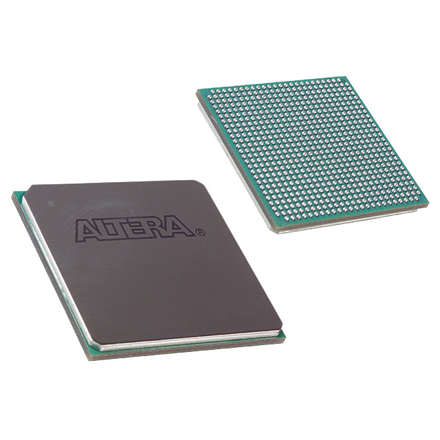
10AX016C4U19E3LG
| Part Description |
Arria 10 GX Field Programmable Gate Array (FPGA) IC 240 10086400 160000 484-BFBGA |
|---|---|
| Quantity | 275 Available (as of June 18, 2026) |

| Product Category | Field Programmable Gate Array (FPGA) |
|---|---|
| Manufacturer | Intel |
| Manufacturing Status | Active |
| Manufacturer Standard Lead Time | 12 Weeks |
| Datasheet |
Specifications & Environmental
| Device Package | 484-UBGA (19x19) | Grade | Extended | Operating Temperature | 0°C – 100°C | ||
|---|---|---|---|---|---|---|---|
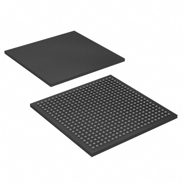
| Package / Case | 484-BFBGA | Number of I/O | 240 | Voltage | 870 mV - 930 mV | ||
| Mounting Method | Surface Mount | RoHS Compliance | RoHS Compliant | REACH Compliance | REACH Unaffected | ||
| Moisture Sensitivity Level | 3 (168 Hours) | Number of LABs/CLBs | 61510 | Number of Logic Elements/Cells | 160000 | ||
| Number of Gates | N/A | ECCN | 5A002A1 | HTS Code | 8542.39.0001 | ||
| Qualification | N/A | Total RAM Bits | 10086400 |
Overview of 10AX016C4U19E3LG – Arria 10 GX FPGA, 160,000 logic elements, 10,086,400-bit RAM
The 10AX016C4U19E3LG is an Intel Arria 10 GX field-programmable gate array (FPGA) in a 484-BFBGA package. Built on the Arria 10 device family architecture, it targets high-performance, power-efficient mid-range applications that require substantial logic capacity, embedded memory, and flexible high-speed connectivity.
Typical market applications include wireless infrastructure, wireline communications, broadcast, computing and storage, medical imaging, and defense systems where a combination of logic density, on-chip memory, and serial connectivity are required.
Key Features
- Core Logic 160,000 logic elements provide programmable capacity for complex digital designs and custom processing pipelines.
- Embedded Memory 10,086,400 total RAM bits of on-chip memory to support large buffering, caching, and real-time data processing.
- I/O and Connectivity 240 I/O pins for flexible external interfacing; Arria 10 family features include support for PCIe Gen1/Gen2/Gen3 hard IP, 10 Gbps Ethernet and advanced serial transceiver capabilities as described in the device overview.
- DSP and Timing Variable-precision DSP blocks and comprehensive clock networks with PLL clock sources support high-throughput signal processing and precision timing architectures.
- Reconfiguration and Reliability Device family features include dynamic and partial reconfiguration, SEU error detection and correction mechanisms, and power management options described in the Arria 10 documentation.
- Power Supply Specified core supply range of 0.870 V to 0.930 V for the device core power rail.
- Package and Mounting Surface-mount 484-BFBGA (supplier package listed as 484-UBGA 19×19) for board-level integration in compact systems.
- Operating Range Extended grade with an operating temperature range of 0 °C to 100 °C.
Typical Applications
- Wireless infrastructure Channel and switch cards in remote radio heads and mobile backhaul designs leveraging on-chip DSP and serial transceivers for high-throughput RF processing and fronthaul transport.
- Wireline communications 40G/100G muxponders, transponders and line cards that utilize PCIe and high-speed serial interfaces alongside significant logic and memory resources.
- Broadcast and media Studio switches, transport and professional video processing that benefit from large embedded RAM for buffering and Arria 10 timing resources for synchronized data streams.
- Computing and storage Flash cache, server acceleration and cloud infrastructure functions that require programmable logic, on-chip memory, and high-speed host interfaces.
- Medical and defense systems Diagnostic imaging and radar/communication systems that need dense logic, DSP capability, and reconfigurability for evolving algorithms.
Unique Advantages
- High logic capacity: 160,000 logic elements enable implementation of complex algorithms, custom accelerators, and multi-function designs on a single device.
- Large on-chip memory: 10,086,400 bits of embedded RAM reduce reliance on external memory for many buffering and caching tasks, simplifying board-level designs.
- Flexible I/O and connectivity: 240 I/O pins combined with Arria 10 family support for high-speed serial interfaces and hard IP blocks streamline high-bandwidth system integration.
- Power-aware architecture: Arria 10 family documentation highlights power-efficiency features; the device’s 0.87–0.93 V core supply specification supports low-voltage operation.
- Reconfiguration and reliability: Support for dynamic and partial reconfiguration and SEU detection/correction improves uptime and enables in-field updates without full system reset.
- System-friendly package and grade: Surface-mount 484-BFBGA packaging and extended 0 °C–100 °C operating range facilitate deployment in a wide range of commercial and industrial-adjacent systems.
Why Choose 10AX016C4U19E3LG?
The 10AX016C4U19E3LG combines a high logic element count, multi-megabit on-chip RAM, and broad I/O flexibility in an Arria 10 GX device package. It is positioned for mid-range designs that require a balance of performance, power efficiency, and reconfigurability—making it suitable for communications, broadcast, compute acceleration, and imaging applications.
Engineers selecting this device benefit from the Arria 10 family’s documented capabilities—DSP blocks, clocking and PLL resources, serial transceivers, and configuration features—backed by Intel’s device documentation and design guidance for integration and long-term maintenance.
Request a quote or submit an inquiry to receive pricing, availability, and additional technical support for 10AX016C4U19E3LG.


Date Founded: 1968
Headquarters: Santa Clara, California, USA
Employees: 130,000+
Revenue: $54.23 Billion
Certifications and Memberships: ISO9001:2015, ISO14001:2015, ISO17025:2017, ISO27001:2022, ISO45001:2018, ISO50001:2018


