
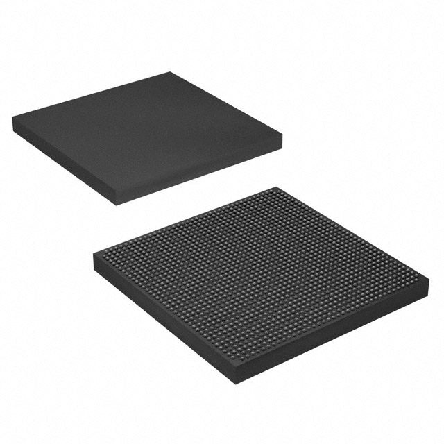
10AX066K2F35I2LG
| Part Description |
Arria 10 GX Field Programmable Gate Array (FPGA) IC 396 49610752 660000 1152-BBGA, FCBGA |
|---|---|
| Quantity | 1,764 Available (as of June 15, 2026) |

| Product Category | Field Programmable Gate Array (FPGA) |
|---|---|
| Manufacturer | Intel |
| Manufacturing Status | Active |
| Manufacturer Standard Lead Time | 9 Weeks |
| Datasheet |
Specifications & Environmental
| Device Package | 1152-FCBGA (35x35) | Grade | Industrial | Operating Temperature | -40°C – 100°C | ||
|---|---|---|---|---|---|---|---|
| Package / Case | 1152-BBGA, FCBGA | Number of I/O | 396 | Voltage | 870 mV - 980 mV | ||
| Mounting Method | Surface Mount | RoHS Compliance | RoHS Compliant | REACH Compliance | REACH Unaffected | ||
| Moisture Sensitivity Level | 3 (168 Hours) | Number of LABs/CLBs | 250540 | Number of Logic Elements/Cells | 660000 | ||
| Number of Gates | N/A | ECCN | 3A001A7B | HTS Code | 8542.39.0001 | ||
| Qualification | N/A | Total RAM Bits | 49610752 |
Overview of 10AX066K2F35I2LG – Arria 10 GX FPGA, 660,000 logic elements, 1152‑FCBGA (35×35)
The 10AX066K2F35I2LG is an Intel Arria 10 GX field‑programmable gate array in a 1152‑FCBGA (35×35) surface‑mount package. It delivers high logic density and substantial on‑chip memory for mid‑range, performance‑sensitive applications in industrial environments.
With 660,000 logic elements, 49,610,752 total RAM bits and 396 I/O, this device is intended for designs that require dense programmable logic, large embedded memory capacity, and broad I/O connectivity while operating across an industrial temperature range.
Key Features
- Logic Capacity — 660,000 logic elements for complex programmable logic and system integration.
- Embedded Memory — 49,610,752 total RAM bits to support large buffering, caching, and on‑chip data structures.
- I/O Count — 396 user I/O pins to accommodate broad peripheral and interface requirements.
- Package & Mounting — 1152‑FCBGA (35×35) surface‑mount package suitable for compact, board‑level integration.
- Power Supply Range — Core supply specified from 870 mV to 980 mV for predictable operating voltage planning.
- Temperature Grade — Industrial operating temperature range of -40 °C to 100 °C for deployment in demanding environments.
- RoHS Compliance — Device is RoHS compliant.
Typical Applications
- Wireless Infrastructure — Use in remote radio head channel processing and mobile backhaul equipment where high logic density and on‑chip memory support signal processing tasks.
- Wireline Telecom — Suited for 40G/100G muxponder, transponder and line‑card designs that require programmable logic and substantial buffering.
- Broadcast & Pro AV — Integration in studio switches and video transport systems benefiting from the device’s I/O count and embedded RAM for stream handling.
- Compute & Storage Acceleration — Applied in server acceleration and flash cache controller designs that need high logic capacity and memory resources.
- Medical Imaging & Diagnostic — Employed in diagnostic imaging subsystems where large on‑chip memory and rugged temperature capability are required.
Unique Advantages
- High Logic Density: 660,000 logic elements enable consolidation of complex functions into a single FPGA, reducing board‑level component count.
- Substantial Embedded Memory: Nearly 49.7 million RAM bits support large buffers and on‑chip data processing, minimizing external memory dependence.
- Comprehensive I/O Capacity: 396 I/O pins provide flexibility for interfacing multiple high‑speed peripherals and control signals.
- Industrial Temperature Rating: Rated from -40 °C to 100 °C for reliable operation in harsh and industrial environments.
- Compact FCBGA Package: 1152‑FCBGA (35×35) allows dense board layouts and surface‑mount assembly for space‑constrained systems.
- Low‑Voltage Core: Core supply range of 870 mV–980 mV enables well‑defined power budgeting for system design.
Why Choose 10AX066K2F35I2LG?
The 10AX066K2F35I2LG positions itself as a high‑density, mid‑range FPGA option for designs that require a balance of programmable logic, significant embedded memory, and extensive I/O in an industrial‑grade package. Its specification set supports integration of complex functions and on‑chip data handling, making it well suited to communications, broadcast, compute acceleration, and medical imaging applications.
Backed by Intel’s Arria 10 device family documentation and development resources, this device offers a clear upgrade path within the Arria 10 portfolio and predictable design parameters for teams focused on scalability and long‑term deployment.
Request a quote or submit an inquiry to receive pricing and availability for the 10AX066K2F35I2LG.


Date Founded: 1968
Headquarters: Santa Clara, California, USA
Employees: 130,000+
Revenue: $54.23 Billion
Certifications and Memberships: ISO9001:2015, ISO14001:2015, ISO17025:2017, ISO27001:2022, ISO45001:2018, ISO50001:2018


