
10AX090U2F45E2SG
| Part Description |
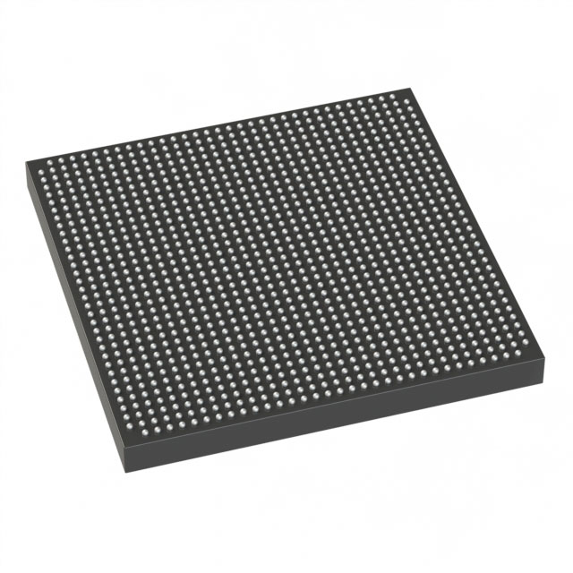
Arria 10 GX Field Programmable Gate Array (FPGA) IC 480 59234304 900000 1932-BBGA, FCBGA |
|---|---|
| Quantity | 570 Available (as of June 10, 2026) |

| Product Category | Field Programmable Gate Array (FPGA) |
|---|---|
| Manufacturer | Intel |
| Manufacturing Status | Active |
| Manufacturer Standard Lead Time | 16 Weeks |
| Datasheet |
Specifications & Environmental
| Device Package | 1932-FCBGA (45x45) | Grade | Extended | Operating Temperature | 0°C – 100°C | ||
|---|---|---|---|---|---|---|---|
| Package / Case | 1932-BBGA, FCBGA | Number of I/O | 480 | Voltage | 870 mV - 980 mV | ||
| Mounting Method | Surface Mount | RoHS Compliance | RoHS Compliant | REACH Compliance | REACH Unaffected | ||
| Moisture Sensitivity Level | 3 (168 Hours) | Number of LABs/CLBs | 339620 | Number of Logic Elements/Cells | 900000 | ||
| Number of Gates | N/A | ECCN | 3A001A7A | HTS Code | 8542.39.0001 | ||
| Qualification | N/A | Total RAM Bits | 59234304 |
Overview of 10AX090U2F45E2SG – Arria 10 GX FPGA, 900,000 Logic Elements, 1932‑FCBGA (45×45)
The 10AX090U2F45E2SG is an Intel Arria 10 GX field programmable gate array (FPGA) IC offering high logic capacity and a broad set of on‑chip resources for mid‑range, performance‑sensitive designs. As part of the Arria 10 family of 20 nm devices, this FPGA targets applications that require a balance of performance and power efficiency across communications, broadcast, computing, and imaging markets.
With 900,000 logic elements, 59,234,304 total RAM bits and 480 I/Os in a 1932‑FCBGA package, this device is designed to integrate large, complex digital functions into a single surface‑mount package while supporting advanced serial protocols and memory interfaces described across the Arria 10 series.
Key Features
- Core Architecture Arria 10 GX series device architecture implemented in a 20 nm process (Arria 10 family); optimized for mid‑range, power‑sensitive applications as described for the device family.
- Logic Capacity 900,000 logic elements for implementing large custom logic, control paths, and hardware accelerators.
- On‑Chip Memory 59,234,304 total RAM bits provide substantial embedded memory for buffering, lookup tables, and on‑chip storage.
- I/O and High‑Speed Interfaces 480 user I/Os to support wide parallel interfaces and board‑level connectivity; the Arria 10 family also documents support for PCIe Gen1/2/3 hard IP, low‑power serial transceivers, and 10 Gbps Ethernet/Interlaken use cases.
- Power and Voltage Supply voltage range of 870 mV to 980 mV to align power‑rail design and system power management strategies.
- Package & Mounting 1932‑BBGA (1932‑FCBGA, 45×45) surface‑mount package for high pin‑count board designs requiring compact, high‑density FPGA integration.
- Operating Range & Grade Extended grade device with an operating temperature range of 0 °C to 100 °C for deployments within this specified thermal window.
Typical Applications
- Wireless Infrastructure Channel cards, remote radio head modules, and mobile backhaul equipment that require programmable logic density and moderate power consumption.
- Wireline & Optical Networking Line cards, muxponder/transponder functions and aggregation systems that can leverage the device’s logic capacity and on‑chip memory for packet processing and protocol offload.
- Broadcast & Professional AV Studio switches and video processing nodes where large logic and memory resources support real‑time media processing and switching.
- Computing & Storage Acceleration Server acceleration, flash cache controllers and cloud compute offload where custom logic and embedded memory accelerate data paths.
- Medical Imaging & Diagnostic Equipment Imaging pipelines and signal processing stages that benefit from high logic counts and substantial on‑chip RAM.
Unique Advantages
- High logic density: 900,000 logic elements enable consolidation of complex logic and multiple functions into a single FPGA, reducing system BOM and board area.
- Large embedded memory: 59,234,304 RAM bits provide ample on‑chip storage for buffering, lookup tables, and intermediate processing without external memory for many use cases.
- Broad I/O capability: 480 I/Os support wide parallel interfaces and flexible board connectivity, simplifying integration with peripherals and memory interfaces.
- Advanced protocol support in the device family: Arria 10 series documentation includes PCIe Gen1/2/3 hard IP and high‑speed serial transceiver support, enabling implementation of modern interconnects and network functions.
- Compact high‑pin package: 1932‑FCBGA (45×45) offers a high pin count in a single surface‑mount package suitable for dense, high‑performance PCB layouts.
- Designed for power‑aware systems: Family documentation highlights power efficiency features and the device operates within a defined core voltage window (870 mV–980 mV) to support controlled power design.
Why Choose 10AX090U2F45E2SG?
The 10AX090U2F45E2SG positions itself as a high‑capacity, mid‑range FPGA option within the Intel Arria 10 GX family, combining 900,000 logic elements, extensive on‑chip RAM and a high I/O count inside a 1932‑FCBGA package. This combination makes it suitable for designs that require significant programmable logic, embedded memory, and flexible interface support without spreading functionality across multiple devices.
For engineering teams building communications, broadcast, compute acceleration, or imaging systems, this device offers a balance of integration density, documented high‑speed interface support in the Arria 10 family, and extended operating grade backed by Intel’s device documentation and ecosystem.
Request a quote or submit an inquiry to evaluate the 10AX090U2F45E2SG for your next design and to obtain pricing, availability, and additional technical support documentation.


Date Founded: 1968
Headquarters: Santa Clara, California, USA
Employees: 130,000+
Revenue: $54.23 Billion
Certifications and Memberships: ISO9001:2015, ISO14001:2015, ISO17025:2017, ISO27001:2022, ISO45001:2018, ISO50001:2018


