
10AX115N2F45E2SG
| Part Description |
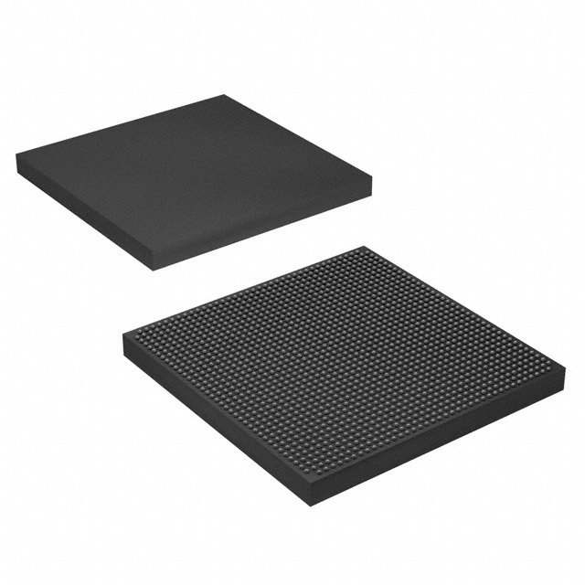
Arria 10 GX Field Programmable Gate Array (FPGA) IC 768 68857856 1150000 1932-BBGA, FCBGA |
|---|---|
| Quantity | 893 Available (as of June 10, 2026) |

| Product Category | Field Programmable Gate Array (FPGA) |
|---|---|
| Manufacturer | Intel |
| Manufacturing Status | Active |
| Manufacturer Standard Lead Time | 16 Weeks |
| Datasheet |
Specifications & Environmental
| Device Package | 1932-FCBGA (45x45) | Grade | Extended | Operating Temperature | 0°C – 100°C | ||
|---|---|---|---|---|---|---|---|
| Package / Case | 1932-BBGA, FCBGA | Number of I/O | 768 | Voltage | 870 mV - 980 mV | ||
| Mounting Method | Surface Mount | RoHS Compliance | RoHS Compliant | REACH Compliance | REACH Unaffected | ||
| Moisture Sensitivity Level | 3 (168 Hours) | Number of LABs/CLBs | 427200 | Number of Logic Elements/Cells | 1150000 | ||
| Number of Gates | N/A | ECCN | 3A001A7A | HTS Code | 8542.39.0001 | ||
| Qualification | N/A | Total RAM Bits | 68857856 |
Overview of 10AX115N2F45E2SG – Arria 10 GX Field Programmable Gate Array (FPGA), 1932-FCBGA
The 10AX115N2F45E2SG is an Intel Arria 10 GX series Field Programmable Gate Array supplied in a 1932-FCBGA (45×45) surface-mount package. As a member of the Arria 10 device family, it leverages the family’s 20 nm mid-range FPGA architecture to deliver a balance of high logic capacity and power efficiency for complex, midrange applications.
With 1,150,000 logic elements, 68,857,856 total RAM bits and 768 user I/Os, this device targets communications, compute, broadcast and imaging applications that require large on-chip logic and memory resources combined with high I/O density.
Key Features
- Core Logic — 1,150,000 logic elements provide a large programmable fabric for complex logic, control and datapath implementations.
- Embedded Memory — 68,857,856 total RAM bits support extensive on-chip buffering, caching and state storage to minimize external memory dependence.
- I/O and Package — 768 user I/Os in a 1932-FCBGA (45×45) package; surface-mount mounting simplifies board-level integration while delivering a high pin count.
- Power Supply & Efficiency — Device supply range 870 mV to 980 mV; Arria 10 family documentation highlights power-efficiency features and power management capabilities.
- Temperature & Grade — Extended grade device with an operating temperature range of 0 °C to 100 °C for applications requiring broader-than-commercial thermal tolerance.
- Advanced On‑Chip Resources — Family-level features include variable-precision DSP blocks, flexible clock networks and PLL clock sources for high-performance signal processing and timing control.
- High-Speed Interfaces and SoC Options — Arria 10 family documentation describes low‑power serial transceivers, PCIe hard IP and SoC integration capabilities (Hard Processor System) for advanced I/O and subsystem integration.
- Standards Compliance — RoHS compliant.
Typical Applications
- Wireless Infrastructure — Channel cards, remote radio head designs and mobile backhaul systems that require dense logic and high I/O connectivity.
- Wireline and Optical Networking — Line cards, muxponders and transponders for 40G/100G systems where on-chip buffering and high-speed interfaces are needed.
- Broadcast and Professional AV — Studio switches, video transport and conferencing equipment benefiting from integrated logic, memory and high I/O counts.
- Compute and Storage Acceleration — Flash cache, server acceleration and cloud compute functions that leverage large logic and embedded memory.
- Medical and Imaging — Diagnostic imaging and scanner subsystems that require on-chip processing, memory and deterministic I/O.
Unique Advantages
- High logic capacity: 1,150,000 logic elements enable implementation of large, complex designs on a single device to reduce system-level part counts.
- Large on-chip memory: 68,857,856 total RAM bits provide substantial internal storage for buffers, frame memory and algorithm state, reducing external memory bandwidth requirements.
- High I/O density: 768 user I/Os support dense connectivity to peripherals, memory devices and high-speed interfaces without sacrificing board layout flexibility.
- Compact, high-pin-count package: 1932-FCBGA (45×45) packaging delivers a high pin count in a compact footprint for space-constrained systems.
- Energy-aware operation: 870 mV to 980 mV supply range and family-level power-saving technologies help manage system power in constrained environments.
- Extended operating range: Extended grade rating and 0 °C to 100 °C operating temperature accommodate broader thermal conditions than typical commercial-only devices.
Why Choose 10AX115N2F45E2SG?
The 10AX115N2F45E2SG positions itself as a high-capacity, midrange FPGA solution for applications that demand extensive logic, abundant embedded memory and high I/O counts in a single package. Its Arria 10 family architecture combines performance-oriented resources such as variable-precision DSP blocks and flexible clocking with documented power-efficiency features and high-speed interface options.
This device is suited for designers building communication systems, broadcast equipment, compute accelerators and imaging systems who need scalable on-chip resources and a compact, high-pin-count package. Supportive device documentation and family-level resources can help accelerate hardware and software development and long-term deployment planning.
Request a quote or submit your configuration and volume requirements to receive pricing and availability information for the 10AX115N2F45E2SG.


Date Founded: 1968
Headquarters: Santa Clara, California, USA
Employees: 130,000+
Revenue: $54.23 Billion
Certifications and Memberships: ISO9001:2015, ISO14001:2015, ISO17025:2017, ISO27001:2022, ISO45001:2018, ISO50001:2018


