
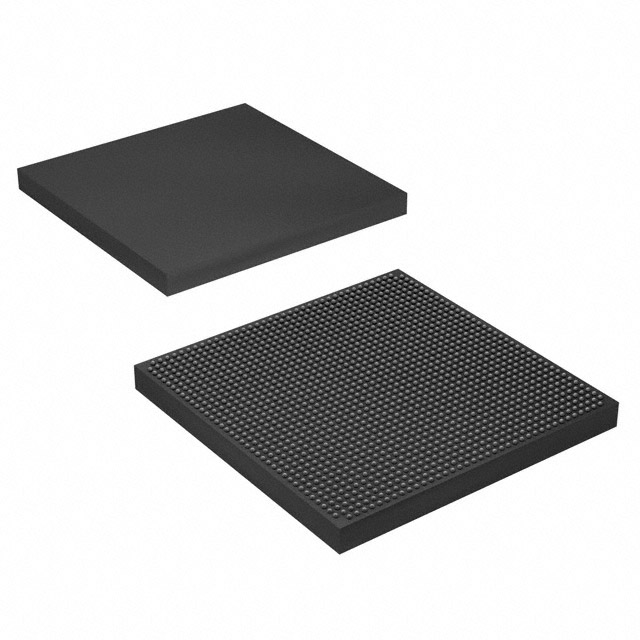
10AX115R2F40E2SG
| Part Description |
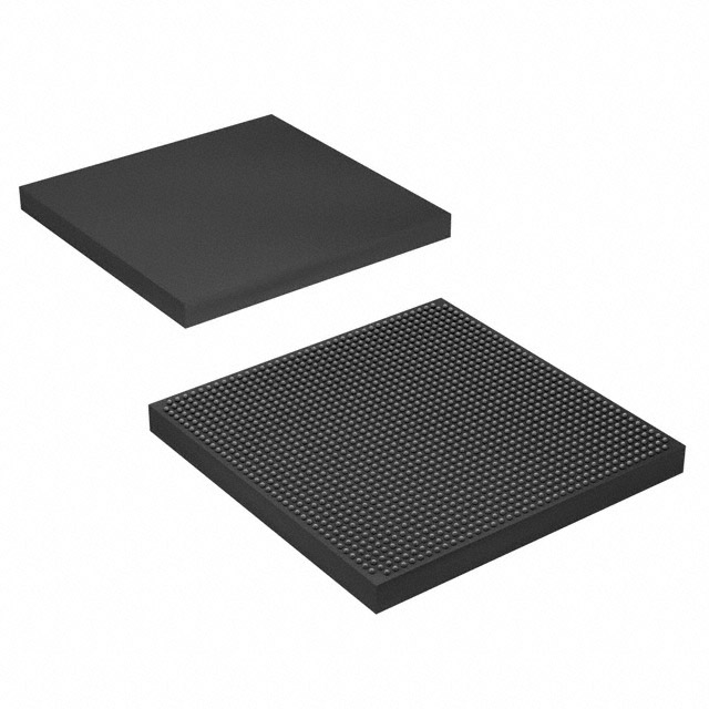
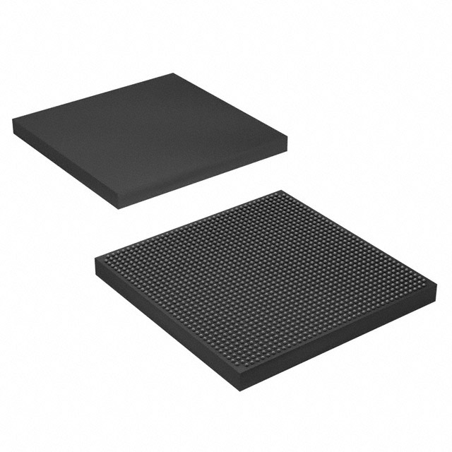
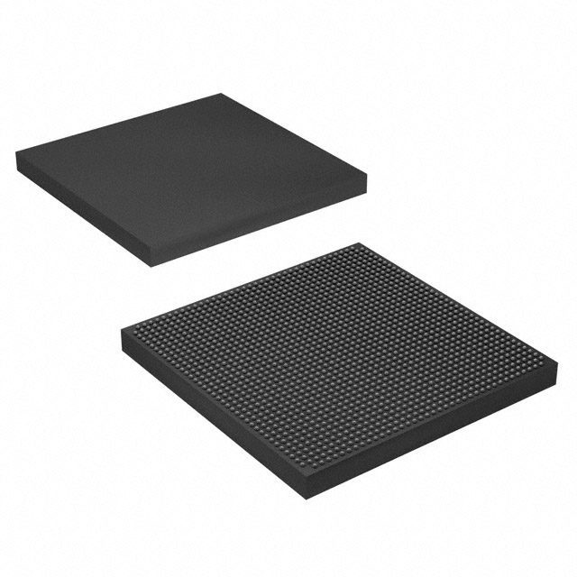
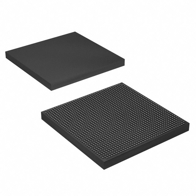
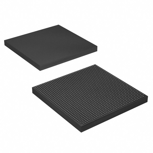
Arria 10 GX Field Programmable Gate Array (FPGA) IC 342 68857856 1150000 1517-BBGA, FCBGA |
|---|---|
| Quantity | 648 Available (as of October 8, 2026) |
| Product Category | Field Programmable Gate Array (FPGA) |
|---|---|
| Manufacturer | Intel |
| Manufacturing Status | Active |
| Manufacturer Standard Lead Time | 16 Weeks |
| Datasheet |
Specifications & Environmental
| Device Package | 1517-FCBGA (40x40) | Grade | Extended | Operating Temperature | 0°C – 100°C | ||
|---|---|---|---|---|---|---|---|
| Package / Case | 1517-BBGA, FCBGA | Number of I/O | 342 | Voltage | 870 mV - 980 mV | ||
| Mounting Method | Surface Mount | RoHS Compliance | RoHS Compliant | REACH Compliance | REACH Unaffected | ||
| Moisture Sensitivity Level | 3 (168 Hours) | Number of LABs/CLBs | 427200 | Number of Logic Elements/Cells | 1150000 | ||
| Number of Gates | N/A | ECCN | 3A001A7A | HTS Code | 8542.39.0001 | ||
| Qualification | N/A | Total RAM Bits | 68857856 |
Overview of 10AX115R2F40E2SG – Arria 10 GX Field Programmable Gate Array (1517-FCBGA)
The 10AX115R2F40E2SG is an Arria 10 GX field programmable gate array (FPGA) in a 1517-FCBGA package. It is a 20 nm mid-range FPGA family device designed for performance and power-efficient system designs.
Targeted at wireless, wireline, broadcast, computing, medical and military markets, this device combines high logic density, large on-chip memory and broad I/O capability to address mid-range, power-sensitive applications.
Key Features
- Core Logic 1,150,000 logic elements (cells) and 427,200 LABs/CLBs equivalent density for complex programmable logic and control functions.
- Embedded Memory 68,857,856 total on-chip RAM bits to support large buffering, caching and on-chip data storage.
- I/O Capacity and Package 342 I/O pins in a 1517-BBGA / 1517-FCBGA (40×40) surface-mount package for flexible board-level connectivity.
- Transceivers and Interfaces Device family overview lists support for high-speed interfaces including PCIe Gen1/Gen2/Gen3 hard IP and 10 Gbps Ethernet / Interlaken-capable PCS and PMA features.
- Power and Voltage Supported core voltage range of 870 mV to 980 mV and power-efficient architecture described for Arria 10 devices.
- Package and Mounting 1517-FCBGA (40×40) surface-mount package optimized for high-pin-count system implementations.
- Operating Range and Grade Extended grade device with an operating temperature range of 0 °C to 100 °C and RoHS compliance.
- Configuration and System Features Family documentation highlights capabilities such as dynamic and partial reconfiguration, clock networks and PLL clock sources for flexible system design.
Typical Applications
- Wireless Infrastructure Channel and switch cards in remote radio heads and mobile backhaul systems benefiting from high logic density and on-chip memory.
- Wireline Networking 40G/100G muxponders, transponders and line cards where high-speed interface hard IP and programmable logic accelerate packet processing.
- Broadcast and Pro AV Studio switches and professional audio/video transport leveraging dense logic and large RAM for media processing and buffering.
- Computing and Storage Flash cache, cloud server acceleration and server transport functions that require on-chip memory and programmable acceleration.
- Medical and Imaging Diagnostic imaging and scanner control that use high logic capacity and reconfiguration features for algorithm acceleration.
Unique Advantages
- High logic density: 1,150,000 logic elements enable complex algorithms and large-scale programmable designs without external ASICs.
- Substantial on-chip memory: Nearly 69 million RAM bits provide ample internal buffering and cache for high-throughput data paths.
- Broad I/O in a compact package: 342 I/O in a 1517-FCBGA (40×40) package supports rich board-level connectivity while keeping PCB footprint controlled.
- Designed for power efficiency: Arria 10 family documentation cites power-saving technologies and a 20 nm process to help manage system power budgets.
- Flexible high-speed interfaces: Family-level support for PCIe Gen1/Gen2/Gen3 and 10 Gbps Ethernet/Interlaken primitives enables integration of common high-bandwidth links.
- Extended operating range: 0 °C to 100 °C grade suits a wide range of commercial and industrial-adjacent applications requiring moderate temperature tolerance.
Why Choose 10AX115R2F40E2SG?
The 10AX115R2F40E2SG delivers a blend of high logic capacity, extensive on-chip memory and versatile I/O in a 1517-FCBGA package, making it suitable for mid-range, performance- and power-sensitive designs. Its Arria 10 GX family characteristics—including support for high-speed interfaces, dynamic reconfiguration and power-saving features—help system designers implement complex functions while managing power and board area.
This device is aimed at engineers and teams developing wireless and wireline infrastructure, broadcast systems, compute/storage accelerators and imaging equipment who need scalable programmable logic with substantial local memory and flexible connectivity.
Request a quote or submit your requirements to receive pricing and availability for the 10AX115R2F40E2SG. Our team will respond with a tailored proposal to support your design timeline.





















Date Founded: 1968
Headquarters: Santa Clara, California, USA
Employees: 130,000+
Revenue: $54.23 Billion
Certifications and Memberships: ISO9001:2015, ISO14001:2015, ISO17025:2017, ISO27001:2022, ISO45001:2018, ISO50001:2018


