
10AX115R2F40I2SGE2
| Part Description |
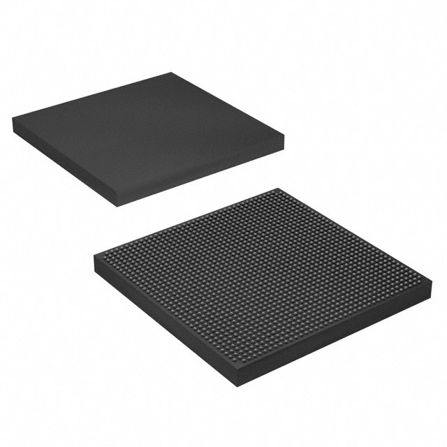
Arria 10 GX Field Programmable Gate Array (FPGA) IC 342 68857856 1150000 1517-BBGA, FCBGA |
|---|---|
| Quantity | 302 Available (as of June 15, 2026) |

| Product Category | Field Programmable Gate Array (FPGA) |
|---|---|
| Manufacturer | Intel |
| Manufacturing Status | Discontinued |
| Manufacturer Standard Lead Time | 6 Weeks |
| Datasheet |
Specifications & Environmental
| Device Package | 1517-FCBGA (40x40) | Grade | Industrial | Operating Temperature | -40°C – 100°C | ||
|---|---|---|---|---|---|---|---|
| Package / Case | 1517-BBGA, FCBGA | Number of I/O | 342 | Voltage | 870 mV - 980 mV | ||
| Mounting Method | Surface Mount | RoHS Compliance | RoHS Compliant | REACH Compliance | REACH Unaffected | ||
| Moisture Sensitivity Level | 3 (168 Hours) | Number of LABs/CLBs | 427200 | Number of Logic Elements/Cells | 1150000 | ||
| Number of Gates | N/A | ECCN | 3A001A7A | HTS Code | 8542.39.0001 | ||
| Qualification | N/A | Total RAM Bits | 68857856 |
Overview of 10AX115R2F40I2SGE2 – Arria 10 GX FPGA, 1517‑FCBGA (40×40)
The 10AX115R2F40I2SGE2 is an Intel Arria 10 GX field programmable gate array (FPGA) in a 1517‑ball FCBGA surface‑mount package. Built on the Intel Arria 10 device family architecture (20 nm), this device combines high logic density, substantial on‑chip RAM, and extensive I/O to address midrange, performance‑sensitive applications.
With 1,150,000 logic element cells, 68,857,856 total RAM bits, and 342 I/O pins, the device targets markets such as wireless and wireline communications, broadcast and professional video, computing and storage acceleration, and other industrial systems that require programmable logic and flexible I/O. It is rated for industrial operation and supports core voltage operation between 870 mV and 980 mV.
Key Features
- Logic Capacity — 1,150,000 logic element cells providing high programmable logic density for complex implementations.
- Logic Blocks — 427,200 logic blocks for partitioning large designs and supporting parallel datapaths.
- Embedded Memory — 68,857,856 total RAM bits to implement large on‑chip buffers, FIFOs, and on‑device data storage.
- I/O and Packaging — 342 device I/Os in a 1517‑ball FCBGA (1517‑BBGA) surface‑mount package (supplier package: 1517‑FCBGA (40×40)).
- Power and Temperature — Core supply range 870 mV to 980 mV and industrial operating temperature range of −40 °C to 100 °C.
- Series Capabilities (Arria 10) — Series‑level features include support for embedded memory blocks, variable‑precision DSP blocks and low‑power serial transceivers as described in the Arria 10 device family documentation, enabling configurable signal processing, compute acceleration, and high‑speed serial connectivity.
- Mounting and Compliance — Surface‑mount FCBGA package with RoHS compliance suitable for standard assembly processes.
Typical Applications
- Wireless Infrastructure — Channel and switch cards, remote radio head functions and mobile backhaul implementations that benefit from programmable data‑path and DSP resources.
- Wireline and Networking — 40G/100G line cards, muxponders and transponders where large logic density and on‑chip memory support packet processing and bridging/aggregation tasks.
- Broadcast and Professional Video — Studio switching, transport and video processing systems leveraging flexible I/O and embedded memory for frame buffering and stream management.
- Computing and Storage Acceleration — Server acceleration, flash cache interfaces and cloud compute offload that use programmable logic to tailor acceleration kernels and data paths.
- Medical and Industrial Systems — Diagnostic imaging and industrial control applications that require robust operating temperature range and high integration.
Unique Advantages
- High Logic Density: 1,150,000 logic elements enable implementation of large, complex designs without external ASICs.
- Substantial On‑Chip Memory: Nearly 69 million bits of RAM reduce dependence on external memory for buffering and accelerate data‑intensive tasks.
- Robust Industrial Range: −40 °C to 100 °C operation and RoHS compliance support deployment in industrial environments.
- Flexible I/O and Packaging: 342 I/Os in a 1517‑ball FCBGA surface‑mount package provide broad connectivity while supporting standard PCB assembly.
- Series‑Level DSP and Transceiver Support: Arria 10 family features such as variable‑precision DSP blocks and low‑power serial transceivers enable efficient signal processing and high‑speed link implementations.
- Controlled Core Power Range: Core supply specification (870 mV–980 mV) allows precise power planning for power‑sensitive designs.
Why Choose 10AX115R2F40I2SGE2?
The 10AX115R2F40I2SGE2 positions itself as a high‑capacity, midrange FPGA option within the Intel Arria 10 family, delivering substantial logic and memory resources in an industrial‑rated FCBGA package. Its combination of 1,150,000 logic elements, large embedded RAM, and hundreds of I/Os makes it suitable for designs that require flexible, programmable hardware acceleration and high‑throughput data handling.
Design teams targeting wireless infrastructure, networking, professional video, compute acceleration, or industrial imaging can leverage the Arria 10 family capabilities to scale performance and integrate functions that reduce board‑level complexity and BOM count. The device is supported by Arria 10 device documentation and ecosystem resources for hardware and software development and deployment.
Request a quote or submit a procurement inquiry to receive pricing and availability information for the 10AX115R2F40I2SGE2 Arria 10 GX FPGA.


Date Founded: 1968
Headquarters: Santa Clara, California, USA
Employees: 130,000+
Revenue: $54.23 Billion
Certifications and Memberships: ISO9001:2015, ISO14001:2015, ISO17025:2017, ISO27001:2022, ISO45001:2018, ISO50001:2018


