
10AX115R3F40E2SG
| Part Description |
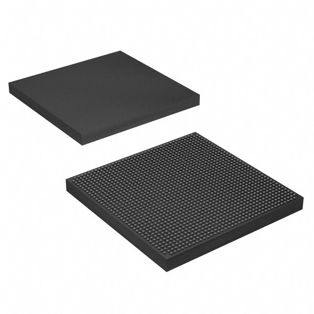
Arria 10 GX Field Programmable Gate Array (FPGA) IC 342 68857856 1150000 1517-BBGA, FCBGA |
|---|---|
| Quantity | 517 Available (as of June 15, 2026) |

| Product Category | Field Programmable Gate Array (FPGA) |
|---|---|
| Manufacturer | Intel |
| Manufacturing Status | Active |
| Manufacturer Standard Lead Time | 16 Weeks |
| Datasheet |
Specifications & Environmental
| Device Package | 1517-FCBGA (40x40) | Grade | Extended | Operating Temperature | 0°C – 100°C | ||
|---|---|---|---|---|---|---|---|
| Package / Case | 1517-BBGA, FCBGA | Number of I/O | 342 | Voltage | 870 mV - 930 mV | ||
| Mounting Method | Surface Mount | RoHS Compliance | RoHS Compliant | REACH Compliance | REACH Unaffected | ||
| Moisture Sensitivity Level | 3 (168 Hours) | Number of LABs/CLBs | 427200 | Number of Logic Elements/Cells | 1150000 | ||
| Number of Gates | N/A | ECCN | 3A001A7A | HTS Code | 8542.39.0001 | ||
| Qualification | N/A | Total RAM Bits | 68857856 |
Overview of 10AX115R3F40E2SG – Arria 10 GX FPGA, 1517-FCBGA
The Intel Arria 10 GX 10AX115R3F40E2SG is a high-performance, power-efficient 20 nm mid-range Field Programmable Gate Array (FPGA) in a 1517-FCBGA (40×40) package. It combines a large programmable fabric with embedded memory, DSP resources and hardened IP to address demanding midrange applications.
Targeted market segments include wireless and wireline infrastructure, broadcast, computing and storage, medical imaging and defense systems where performance, power efficiency and flexible integration are required.
Key Features
- Logic Capacity The device provides 1,150,000 logic elements for complex digital designs and high-density integration.
- Embedded Memory 68,857,856 total RAM bits of on-chip memory to support large buffers, frame storage and memory-intensive algorithms.
- I/O and Packaging 342 user I/Os in a 1517-BBGA (1517-FCBGA, 40×40) surface-mount package for dense board-level integration.
- Power Supply Operates with a core supply range of 870 mV to 930 mV, enabling low-voltage power management strategies.
- Operating Range Specified for 0°C to 100°C operation and supplied in an Extended grade.
- Transceivers and Connectivity Supports low-power serial transceivers and includes hard IP for Ethernet and Interlaken use cases, with documented support for 10 Gbps Ethernet.
- Hard IP and Interfaces Includes PCIe Gen1/Gen2/Gen3 hard IP and enhanced PCS hard IP for high-speed protocols.
- Compute and DSP Variable-precision DSP blocks and adaptive logic modules provide flexible datapath and signal-processing resources.
- Clocking and PLLs Flexible clock networks with fractional synthesis and I/O PLLs for precise timing and multi-clock-domain designs.
- Reconfiguration and Development Device architecture and documentation reference dynamic and partial reconfiguration and support for hardware and software development flows.
Typical Applications
- Wireless Infrastructure Channel and switch cards in remote radio heads and mobile backhaul equipment leveraging the device's performance and DSP resources.
- Wireline Networks 40G/100G muxponders, transponders and line cards where high-speed I/O and hardened protocol IP (PCIe, Ethernet) are required.
- Broadcast and Media Studio switching, videoconferencing and professional audio/video processing using embedded memory and high-density logic.
- Computing & Storage Flash cache, cloud server acceleration and server offload tasks that benefit from large on-chip memory and programmable compute fabric.
- Medical and Defense Systems Diagnostic imaging, radar and electronic warfare applications that require midrange FPGA performance with extended temperature operation.
Unique Advantages
- High logic density: 1,150,000 logic elements enable consolidation of complex functions into a single device, reducing board-level BOM.
- Large on-chip memory: Nearly 69Mbits of RAM supports deep buffering and memory-hungry algorithms without relying solely on external memory.
- Integrated hardened IP: Built-in PCIe Gen1/2/3 and Ethernet/Interlaken PCS hard IP simplify high-speed interface implementation and reduce development time.
- Flexible clocking and transceivers: Fractional synthesis PLLs and low-power serial transceivers provide precise timing and high-speed connectivity options.
- Extended-grade operation: Specified 0°C to 100°C operating range and Extended grade part selection for applications requiring broader temperature range than commercial-only parts.
- Scalable development model: Support for dynamic and partial reconfiguration and documented hardware/software development flows to accelerate system integration.
Why Choose 10AX115R3F40E2SG?
The 10AX115R3F40E2SG Arria 10 GX device positions itself for midrange designs that demand a balance of performance, power efficiency and integration. With a large logic fabric, substantial embedded memory and hardened protocol IP, it is suited to systems that consolidate multiple functions on a single FPGA while maintaining power-conscious operation.
Engineers designing wireless backhaul, high-speed networking, broadcast processing, server acceleration or advanced imaging and defense systems will find the device's combination of logic density, I/O capability and transceiver/connectivity support valuable for scalable, robust designs backed by Intel's device documentation and development ecosystem.
Request a quote or submit an inquiry to receive pricing, availability and ordering information for the 10AX115R3F40E2SG Arria 10 GX FPGA. Our team can provide lead times and support for your procurement and design evaluation needs.


Date Founded: 1968
Headquarters: Santa Clara, California, USA
Employees: 130,000+
Revenue: $54.23 Billion
Certifications and Memberships: ISO9001:2015, ISO14001:2015, ISO17025:2017, ISO27001:2022, ISO45001:2018, ISO50001:2018


