
10AX115R3F40I2SGES
| Part Description |
Arria 10 GX Field Programmable Gate Array (FPGA) IC 342 68857856 1150000 1517-BBGA, FCBGA |
|---|---|
| Quantity | 587 Available (as of June 15, 2026) |

| Product Category | Field Programmable Gate Array (FPGA) |
|---|---|
| Manufacturer | Intel |
| Manufacturing Status | Discontinued |
| Manufacturer Standard Lead Time | 6 Weeks |
| Datasheet |
Specifications & Environmental
| Device Package | 1517-FCBGA (40x40) | Grade | Industrial | Operating Temperature | -40°C – 100°C | ||
|---|---|---|---|---|---|---|---|
| Package / Case | 1517-BBGA, FCBGA | Number of I/O | 342 | Voltage | 870 mV - 930 mV | ||
| Mounting Method | Surface Mount | RoHS Compliance | RoHS Compliant | REACH Compliance | REACH Unaffected | ||
| Moisture Sensitivity Level | 3 (168 Hours) | Number of LABs/CLBs | 427200 | Number of Logic Elements/Cells | 1150000 | ||
| Number of Gates | N/A | ECCN | 3A001A7A | HTS Code | 8542.39.0001 | ||
| Qualification | N/A | Total RAM Bits | 68857856 |
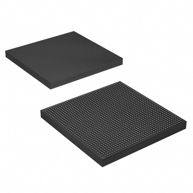
Overview of 10AX115R3F40I2SGES – Arria 10 GX FPGA, 1,150,000 logic elements, 1517-FCBGA
The 10AX115R3F40I2SGES is an Intel Arria 10 GX Field Programmable Gate Array (FPGA) in a 1517-FCBGA (40×40) package. It is a 20 nm-class mid‑range FPGA family member offering high logic density, large embedded memory, and integrated high‑speed I/O suitable for demanding industrial applications.
With 1,150,000 logic elements, 68,857,856 total RAM bits, and 342 I/O pins, this surface‑mount, industrial‑grade device targets applications that require a combination of performance, on‑chip memory and extensive I/O connectivity while operating across an extended temperature range.
Key Features
- Core density — 1,150,000 logic elements to support large, complex designs and dense FPGA implementations.
- Embedded memory — 68,857,856 total RAM bits for on‑chip buffering, data staging, and memory‑intensive functions.
- I/O capacity — 342 I/O pins provided in a 1517‑FCBGA (40×40) package to support broad connectivity and external interfaces.
- High‑speed serial and protocol support — Family documentation lists PCIe Gen1/Gen2/Gen3 hard IP, enhanced PCS hard IP for Interlaken and 10 Gbps Ethernet, and low‑power serial transceivers as supported features.
- Power envelope — Supported supply voltage range from 870 mV to 930 mV for device core power planning.
- Industrial temperature range — Rated to operate from −40 °C to 100 °C for deployment in extended‑temperature environments.
- Package & mounting — 1517‑BBGA/FCBGA package case with surface‑mount mounting type for standard PCB assembly processes.
- Regulatory — RoHS‑compliant component to meet lead‑free manufacturing requirements.
Typical Applications
- Wireless infrastructure — Channel and switch cards in remote radio heads and mobile backhaul designs that need logic density and high‑speed I/O.
- Wireline transport and routing — 40G/100G muxponders, transponders and line cards where on‑chip memory and serial protocol hard IP accelerate packet handling and aggregation.
- Broadcast and professional AV — Studio switches, videoconferencing and professional audio/video processing that benefit from large embedded memory and flexible I/O.
- Computing and storage acceleration — Flash cache, cloud server acceleration and other data–center adjacent functions requiring large logic resources and memory capacity.
- Medical and defense systems — Diagnostic imaging, radar, electronic warfare and secure communications that require industrial temperature operation and high integration.
Unique Advantages
- High logic density: 1,150,000 logic elements enable implementation of complex algorithms and large hardware accelerators on a single device.
- Substantial on‑chip memory: Nearly 69 million RAM bits reduce dependence on external memory for buffering and high‑throughput datapaths.
- Broad I/O and package choice: 342 I/O in a 1517‑FCBGA (40×40) package provides flexibility to interface with multiple peripherals and high‑speed lanes.
- Designed for industrial environments: −40 °C to 100 °C operating range and surface‑mount package support deployment in extended‑temperature systems.
- Integrated protocol hard IP: Family support for PCIe Gen1/2/3 and Ethernet/Interlaken PCS offloads common protocol functions and accelerates time to market.
- RoHS compliant: Conforms to lead‑free manufacturing requirements for modern production processes.
Why Choose 10AX115R3F40I2SGES?
The 10AX115R3F40I2SGES Arria 10 GX FPGA delivers a combination of high logic capacity, large embedded memory, and extensive I/O in a single industrial‑rated FCBGA package. It is positioned for mid‑range designs that require significant on‑chip resources and support for high‑speed serial protocols while maintaining power and thermal considerations through its defined core voltage range.
This device is well suited for engineering teams building wireless and wireline infrastructure, broadcast systems, data‑center acceleration, medical imaging and defense applications that need scalability, integration, and documented family‑level support for protocol hard IP and serial transceivers.
Request a quote or submit a pricing inquiry to learn more about availability and lead times for 10AX115R3F40I2SGES.


Date Founded: 1968
Headquarters: Santa Clara, California, USA
Employees: 130,000+
Revenue: $54.23 Billion
Certifications and Memberships: ISO9001:2015, ISO14001:2015, ISO17025:2017, ISO27001:2022, ISO45001:2018, ISO50001:2018


