
10AX115S2F45E1SG
| Part Description |
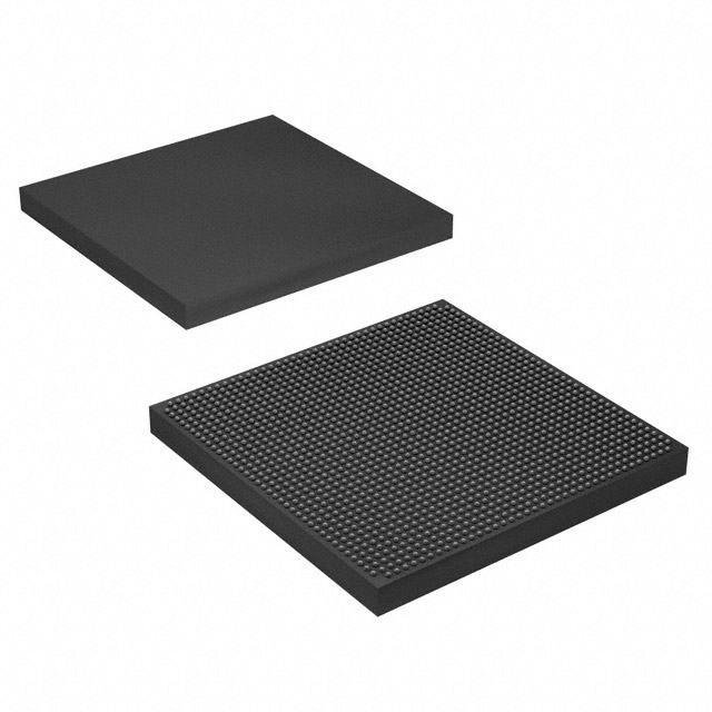
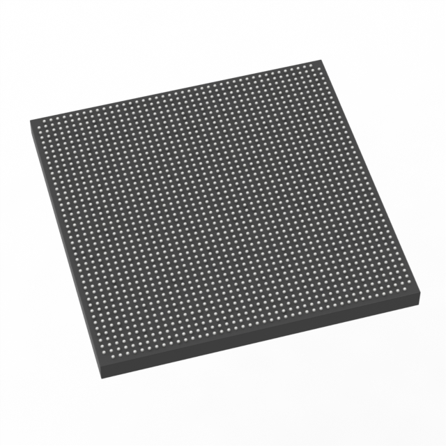
Arria 10 GX Field Programmable Gate Array (FPGA) IC 624 68857856 1150000 1932-BBGA, FCBGA |
|---|---|
| Quantity | 1,058 Available (as of June 15, 2026) |

| Product Category | Field Programmable Gate Array (FPGA) |
|---|---|
| Manufacturer | Intel |
| Manufacturing Status | Active |
| Manufacturer Standard Lead Time | 16 Weeks |
| Datasheet |
Specifications & Environmental
| Device Package | 1932-FCBGA (45x45) | Grade | Extended | Operating Temperature | 0°C – 100°C | ||
|---|---|---|---|---|---|---|---|
| Package / Case | 1932-BBGA, FCBGA | Number of I/O | 624 | Voltage | 870 mV - 980 mV | ||
| Mounting Method | Surface Mount | RoHS Compliance | RoHS Compliant | REACH Compliance | REACH Unaffected | ||
| Moisture Sensitivity Level | 3 (168 Hours) | Number of LABs/CLBs | 427200 | Number of Logic Elements/Cells | 1150000 | ||
| Number of Gates | N/A | ECCN | 3A001A7A | HTS Code | 8542.39.0001 | ||
| Qualification | N/A | Total RAM Bits | 68857856 |
Overview of 10AX115S2F45E1SG – Arria 10 GX FPGA, 1932-FCBGA
The 10AX115S2F45E1SG is an Intel Arria 10 GX Field Programmable Gate Array (FPGA) supplied in a 1932-FCBGA (45×45) package. It delivers a high-density, mid-range FPGA architecture designed for applications that require significant logic, embedded memory, and extensive I/O connectivity.
As part of the Arria 10 device family, this device targets markets such as wireless, wireline, broadcast, computing and storage, medical, and military systems where performance and power efficiency are important design considerations.
Key Features
- Core logic density — 1,150,000 logic elements provide substantial programmable logic resources for complex designs and system integration.
- Embedded memory — 68,857,856 total RAM bits enable large on-chip buffering, datapath storage, and complex state machines without immediate reliance on external memory.
- I/O capacity — 624 user I/O pins support broad peripheral and interface connectivity for multi-channel and multi-protocol designs.
- Power supply — Designed to operate from 870 mV to 980 mV core supply, supporting the device’s power architecture and system power-planning.
- Package & mounting — 1932-BBGA FCBGA package (1932-FCBGA, 45×45) in a surface-mount form factor for high-pin-count, board-level integration.
- Temperature & grade — Extended grade device with an operating temperature range of 0 °C to 100 °C for deployment in controlled industrial and commercial environments.
- Compliance — RoHS compliant.
Typical Applications
- Wireless infrastructure — Channel and switch cards in remote radio heads and mobile backhaul systems that require high logic density and on-chip memory.
- Wireline networking — Line cards, muxponders and transponders for 40G/100G systems where extensive I/O and programmable logic enable protocol handling and packet processing.
- Broadcast and professional A/V — Studio switches and video-processing front ends that benefit from large embedded memory and flexible I/O mapping.
- Computing and storage acceleration — Server and storage acceleration tasks such as cache management and custom offload functions that use dense logic and memory resources.
- Medical and defense systems — Diagnostic imaging, radar, and secure communications requiring configurable logic and substantial on-chip resources.
Unique Advantages
- High logic capacity: 1,150,000 logic elements allow complex algorithms and multi-function systems to be implemented on a single FPGA.
- Large on-chip memory: Nearly 69 million RAM bits reduce dependence on external memory and simplify board-level memory architectures.
- Extensive I/O: 624 I/O pins provide flexibility for high-channel-count interfaces and integration with diverse peripherals.
- Compact, high-pin-count package: 1932-FCBGA (45×45) enables dense routing and accommodates high I/O in a surface-mount form factor.
- Extended-grade operation: Rated for 0 °C to 100 °C operation to meet the needs of commercial and controlled industrial applications.
- RoHS compliant: Supports environmental and regulatory requirements for modern electronic systems.
Why Choose 10AX115S2F45E1SG?
The 10AX115S2F45E1SG is positioned for designs that demand a balance of high logic density, substantial embedded memory, and broad I/O in a single, surface-mount package. Its Arria 10 GX heritage and device-family capabilities make it suitable for mid-range applications across communications, broadcast, storage acceleration, medical imaging, and defense systems.
Choosing this device supports scalable, integrated designs that leverage on-chip resources to reduce external BOM and simplify system architectures while operating within an extended temperature envelope and standard surface-mount packaging.
Request a quote or submit an inquiry to receive pricing, availability, and lead-time information for the 10AX115S2F45E1SG.


Date Founded: 1968
Headquarters: Santa Clara, California, USA
Employees: 130,000+
Revenue: $54.23 Billion
Certifications and Memberships: ISO9001:2015, ISO14001:2015, ISO17025:2017, ISO27001:2022, ISO45001:2018, ISO50001:2018


