
10AX115S2F45E2SG
| Part Description |
Arria 10 GX Field Programmable Gate Array (FPGA) IC 624 68857856 1150000 1932-BBGA, FCBGA |
|---|---|
| Quantity | 826 Available (as of June 15, 2026) |
| Product Category | Field Programmable Gate Array (FPGA) |
|---|---|
| Manufacturer | Intel |
| Manufacturing Status | Active |
| Manufacturer Standard Lead Time | 16 Weeks |
| Datasheet |
Specifications & Environmental
| Device Package | 1932-FCBGA (45x45) | Grade | Extended | Operating Temperature | 0°C – 100°C | ||
|---|---|---|---|---|---|---|---|
| Package / Case | 1932-BBGA, FCBGA | Number of I/O | 624 | Voltage | 870 mV - 980 mV | ||
| Mounting Method | Surface Mount | RoHS Compliance | RoHS Compliant | REACH Compliance | REACH Unaffected | ||
| Moisture Sensitivity Level | 3 (168 Hours) | Number of LABs/CLBs | 427200 | Number of Logic Elements/Cells | 1150000 | ||
| Number of Gates | N/A | ECCN | 3A001A7A | HTS Code | 8542.39.0001 | ||
| Qualification | N/A | Total RAM Bits | 68857856 |
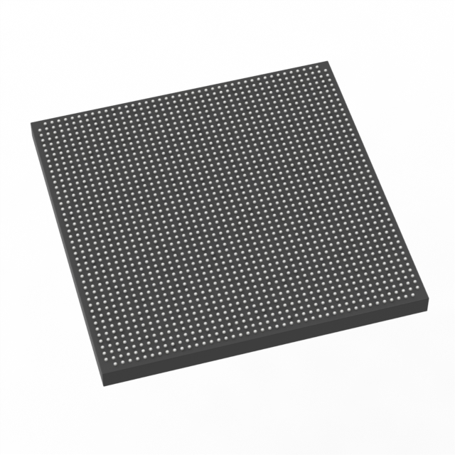
Overview of 10AX115S2F45E2SG – Arria 10 GX FPGA, 1,150,000 logic elements, 1932-FCBGA
The 10AX115S2F45E2SG is an Intel Arria 10 GX field programmable gate array (FPGA) supplied in a 1932‑FCBGA (45×45) package for surface-mount applications. It delivers the Arria 10 family’s combination of high performance and power efficiency for mid-range, power-sensitive designs.
Targeted markets include wireless and wireline communications, broadcast, computing and storage, medical imaging, and military systems. The device couples high logic density, substantial embedded RAM, and extensive I/O to support complex system integration and high-throughput designs.
Key Features
- Core Logic 1,150,000 logic elements provide high implementation density for complex FPGA designs.
- Embedded Memory 68,857,856 total RAM bits for on-chip buffering, frame storage, and algorithm acceleration.
- I/O Capacity 624 device I/O pins to support broad interfacing and multi-channel connectivity.
- Transceiver and Interface IP Arria 10 family features include hard IP for PCIe Gen1/Gen2/Gen3 and support for 10 Gbps Ethernet and other serial protocols (as documented for the Arria 10 series).
- Programmable Fabric and DSP Arria 10 architecture provides adaptive logic modules and variable‑precision DSP blocks (as specified for the device family) to accelerate signal processing and compute tasks.
- Power and Voltage Device supply range 870 mV to 980 mV, reflecting the Arria 10 family’s focus on power-efficient operation.
- Package & Mounting Surface-mount 1932-FCBGA (45×45 mm) package for high‑density board integration.
- Temperature & Grade Extended grade with an operating temperature range of 0 °C to 100 °C.
- Standards & Compliance RoHS compliant.
Typical Applications
- Wireless infrastructure Channel cards, remote radio head control, and baseband processing where high logic density and on-chip memory enable advanced signal processing.
- Wireline networking Line cards, muxponders, and aggregation equipment that require multi‑lane I/O and hard IP for high-speed serial protocols.
- Broadcast and professional video Studio switching, video transport, and conferencing systems that benefit from large on-chip RAM and dense logic for frame buffering and real‑time processing.
- Computing and storage Server acceleration, flash cache control, and cloud compute appliances leveraging DSP resources and programmable fabric.
- Military and defense Radar, EW, and guidance subsystems that use high logic capacity and deterministic FPGA processing (device usage should follow project qualification requirements).
Unique Advantages
- High implementation density: 1,150,000 logic elements enable complex functions and large-scale designs within a single FPGA device.
- Large on-chip memory: 68,857,856 total RAM bits reduce external memory dependency for buffering and data-intensive algorithms.
- Extensive I/O capability: 624 I/O pins accommodate multi-channel interfaces and dense system-level connectivity.
- Power‑aware operation: Narrow supply range (870 mV–980 mV) consistent with Arria 10’s power-efficiency emphasis supports designs where supply optimization is important.
- Production-ready package: 1932‑FCBGA (45×45) surface-mount package delivers a compact, high‑pin‑count solution for PCB integration.
- Documented device family support: Backed by Intel Arria 10 device documentation and handbooks for design guidance and device errata.
Why Choose 10AX115S2F45E2SG?
The 10AX115S2F45E2SG positions itself as a high‑density, mid‑range FPGA for designs that need significant logic resources, on-chip memory, and broad I/O in a single package. Its Arria 10 GX family heritage emphasizes improved performance and power efficiency for power‑sensitive applications.
This device is suited to system designers and procurement teams building complex communications, video, compute acceleration, and defense systems that require scalable FPGA capacity, documented device support, and RoHS compliance.
Request a quote or submit a sales inquiry to evaluate 10AX115S2F45E2SG for your next design and obtain pricing and availability information.


Date Founded: 1968
Headquarters: Santa Clara, California, USA
Employees: 130,000+
Revenue: $54.23 Billion
Certifications and Memberships: ISO9001:2015, ISO14001:2015, ISO17025:2017, ISO27001:2022, ISO45001:2018, ISO50001:2018


