
1SD280PT1F55E1VG
| Part Description |
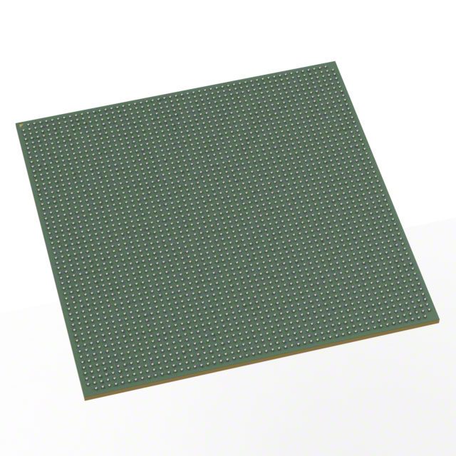
Stratix® 10 DX Field Programmable Gate Array (FPGA) IC 816 240123904 2753000 2912-BBGA, FCBGA |
|---|---|
| Quantity | 355 Available (as of June 9, 2026) |

| Product Category | Field Programmable Gate Array (FPGA) |
|---|---|
| Manufacturer | Intel |
| Manufacturing Status | Active |
| Manufacturer Standard Lead Time | 12 Weeks |
| Datasheet |
Specifications & Environmental
| Device Package | 2912-FBGA (55x55) | Grade | Extended | Operating Temperature | 0°C – 100°C | ||
|---|---|---|---|---|---|---|---|
| Package / Case | 2912-BBGA, FCBGA | Number of I/O | 816 | Voltage | 870 mV - 970 mV | ||
| Mounting Method | Surface Mount | RoHS Compliance | Unknown | REACH Compliance | REACH Unknown | ||
| Moisture Sensitivity Level | 3 (168 Hours) | Number of LABs/CLBs | N/A | Number of Logic Elements/Cells | 2753000 | ||
| Number of Gates | N/A | ECCN | N/A | HTS Code | N/A | ||
| Qualification | N/A | Total RAM Bits | 240123904 |
Overview of 1SD280PT1F55E1VG – Stratix® 10 DX FPGA, 2912-FBGA (55×55), Extended Grade
The 1SD280PT1F55E1VG is a Stratix® 10 DX Field Programmable Gate Array (FPGA) IC from Intel, provided in a 2912-ball FBGA package (55×55). It delivers very large programmable logic and on‑chip memory capacity combined with a high I/O count and an extended-grade operating range for demanding board-level designs.
On-chip resources and interfaces documented for the Stratix 10 DX family—together with published device errata—make this device suitable for designs that require substantial logic density, significant embedded RAM, and broad I/O connectivity while operating within the specified core voltage and temperature envelope.
Key Features
- High Logic Capacity 2,753,000 logic elements (Number Of Logic Elements Cells: 2753000) to implement large, complex FPGA designs.
- Large On‑Chip RAM 240,123,904 total RAM bits (Total Ram Bits: 240123904) for buffering, on-chip storage, and memory‑intensive functions.
- Extensive I/O 816 user I/Os (Number Of Io: 816) to support wide parallel interfaces and dense external connectivity.
- Power Supply Core voltage supply range from 870 mV to 970 mV (Voltage Supply: 870 mV to 970 mV) for defined power-domain design and power sequencing.
- Package and Mounting 2912-BBGA/FCBGA package (Supplier Device Package: 2912-FBGA (55x55)) in a surface-mount form factor (Mounting Type: Surface Mount) for compact board integration.
- Extended Temperature Grade Rated for 0 °C to 100 °C operating temperature (Operating Temperature: 0 C to 100 C) and specified as Extended grade (Grade: Extended).
- Compliance and Documentation RoHS compliant (RoHS Status: Compliant). Product documentation includes Intel Stratix 10 DX device errata covering device‑specific and HPS/processor-related items for the Stratix 10 DX production family.
Typical Applications
- PCIe‑enabled systems — Devices and subsystems that require large logic and memory resources alongside high I/O counts and documented PCIe-related behavior referenced in the Stratix 10 DX errata.
- HPS‑integrated embedded designs — Designs combining FPGA fabric with Hard Processor System (HPS) features where on‑chip RAM and extensive I/O simplify system partitioning and data movement.
- High‑density logic and memory acceleration — Workloads that benefit from millions of logic elements and hundreds of megabits of on‑chip RAM for custom acceleration and buffering.
- Dense I/O systems — Board-level applications requiring hundreds of user I/Os for parallel interfaces, sensors, or wide‑bus connectivity.
Unique Advantages
- Massive programmable fabric: 2,753,000 logic elements enable implementation of very large, complex designs on a single FPGA device, reducing system partitioning.
- Substantial on‑chip memory: 240,123,904 bits of RAM support large buffers, FIFOs, and memory‑centric accelerators without relying solely on external memory.
- Broad connectivity: 816 dedicated I/Os provide flexibility for interfacing to multiple peripherals, parallel buses, and high‑pin‑count modules.
- Compact package integration: 2912‑ball FBGA (55×55) surface‑mount package enables high component density on modern PCBs while delivering extensive I/O and routing resources.
- Documented device behavior: Intel Stratix 10 DX device errata and processor/HPS errata are available for design planning and system validation.
- Controlled power domain: Defined core supply range (870 mV–970 mV) assists in predictable power sequencing and thermal planning.
Why Choose 1SD280PT1F55E1VG?
The 1SD280PT1F55E1VG positions itself as a high-capacity Stratix 10 DX FPGA option when large programmable logic, significant on‑chip RAM, and extensive I/O are primary design drivers. The combination of 2,753,000 logic elements, over 240 million bits of RAM, and 816 I/Os in a 2912‑ball FBGA package supports consolidation of complex functions onto a single device while maintaining a clear power and thermal specification (870 mV–970 mV, 0 °C–100 °C).
Backed by Intel documentation that includes device and processor/HPS errata for the Stratix 10 DX family, this device is suited for engineering teams that require documented device behavior and the on‑chip resources needed to implement large FPGA-based systems.
Request a quote or submit a sales inquiry to receive pricing, availability, and technical details for 1SD280PT1F55E1VG.


Date Founded: 1968
Headquarters: Santa Clara, California, USA
Employees: 130,000+
Revenue: $54.23 Billion
Certifications and Memberships: ISO9001:2015, ISO14001:2015, ISO17025:2017, ISO27001:2022, ISO45001:2018, ISO50001:2018


