
1SD280PT2F55E1VG
| Part Description |
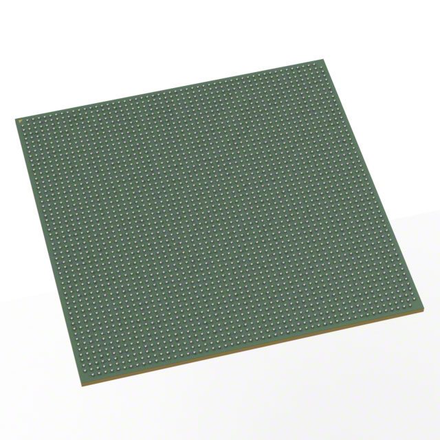
Stratix® 10 DX Field Programmable Gate Array (FPGA) IC 816 240123904 2753000 2912-BBGA, FCBGA |
|---|---|
| Quantity | 593 Available (as of June 15, 2026) |

| Product Category | Field Programmable Gate Array (FPGA) |
|---|---|
| Manufacturer | Intel |
| Manufacturing Status | Active |
| Manufacturer Standard Lead Time | 12 Weeks |
| Datasheet |
Specifications & Environmental
| Device Package | 2912-FBGA (55x55) | Grade | Extended | Operating Temperature | 0°C – 100°C | ||
|---|---|---|---|---|---|---|---|
| Package / Case | 2912-BBGA, FCBGA | Number of I/O | 816 | Voltage | 870 mV - 970 mV | ||
| Mounting Method | Surface Mount | RoHS Compliance | Unknown | REACH Compliance | REACH Unaffected | ||
| Moisture Sensitivity Level | 3 (168 Hours) | Number of LABs/CLBs | N/A | Number of Logic Elements/Cells | 2753000 | ||
| Number of Gates | N/A | ECCN | N/A | HTS Code | N/A | ||
| Qualification | N/A | Total RAM Bits | 240123904 |
Overview of 1SD280PT2F55E1VG – Stratix® 10 DX Field Programmable Gate Array (FPGA) IC, 816 I/O, 2912-BBGA
The 1SD280PT2F55E1VG is a Stratix® 10 DX FPGA device from Intel, delivering a high logic-density fabric with extensive embedded RAM and a large I/O complement. As a member of the Stratix 10 DX family, it leverages the family’s Hyperflex core architecture and advanced packaging and I/O capabilities to address high-performance acceleration use cases.
This device targets markets such as datacenter acceleration, networking, cloud computing and test & measurement where high logic capacity, significant on-chip RAM, and broad connectivity are required. Key value comes from large logic and memory resources, high-speed I/O, and robust package and thermal characteristics suitable for extended-grade deployments.
Key Features
- High Logic Capacity 2,753,000 logic elements (cells) for implementing large, complex FPGA designs.
- Substantial On-Chip RAM 240,123,904 total RAM bits to support large buffering, caching, and on-chip data structures.
- Extensive I/O 816 I/O pins to support dense external interfaces and system integration.
- Stratix 10 DX Architecture Built on the Stratix 10 DX family architecture featuring Intel Hyperflex core concepts and family-level innovations described in the device overview.
- High-Speed Transceiver & Hard IP Capabilities (Family-Level) Family documentation highlights transceivers and hard IP blocks for coherent and non-coherent interfaces, PCIe Gen4 and 100 Gigabit Ethernet—enabling high-throughput system connectivity when implemented for specific devices in the DX series.
- Package and Mounting 2912-BBGA FCBGA package (supplier device package: 2912-FBGA, 55×55) with surface-mount mounting type for compact board-level integration.
- Supply Voltage Core supply range of 870 mV to 970 mV.
- Operating Range & Grade Extended grade with an operating temperature range of 0 °C to 100 °C. RoHS compliant.
Typical Applications
- Datacenter Acceleration Implement high-throughput, low-latency acceleration engines and offload functions using the device’s high logic count and large embedded RAM.
- Networking & Telecom Deploy packet processing, protocol offload, and line-rate interfaces leveraging the family’s high-speed transceiver and hard IP capabilities.
- Cloud Computing Infrastructure Use for programmable data-paths and custom processing tasks where dense logic, memory, and extensive I/O enable scalable deployment.
- Test & Measurement Build high-channel-count capture, analysis, and signal processing systems that benefit from abundant logic elements and on-chip RAM.
Unique Advantages
- Massive Logic & Memory Resources: 2.75M logic elements plus over 240Mbits of on-chip RAM offer capacity for large, complex designs without immediate external memory dependence.
- Broad System Connectivity: 816 I/O pins and family-level support for high-speed transceivers and hardened interface IP enable diverse external interfaces and high-bandwidth links.
- Advanced Packaging: 2912-BBGA FCBGA (55×55) package enables dense integration on modern PCB designs while supporting surface-mount assembly.
- Optimized Power Window: Core supply specification (870 mV–970 mV) supports predictable power design and rail planning for FPGA-based systems.
- Extended Grade Reliability: Rated for 0 °C to 100 °C operation in an Extended grade offering suitable thermal headroom for many high-performance system environments.
- Compliance: RoHS compliant to meet common environmental and manufacturing requirements.
Why Choose 1SD280PT2F55E1VG?
The 1SD280PT2F55E1VG positions itself as a high-capacity Stratix 10 DX FPGA option for designs that require very large logic and embedded RAM resources combined with a high I/O count and advanced family-level connectivity options. It is well suited to engineering teams building datacenter accelerators, networking equipment, cloud infrastructure components, and sophisticated test systems.
Choosing this device offers designers the ability to scale complex implementations within a proven Stratix 10 DX family architecture, while leveraging a compact FCBGA package and defined operating and power characteristics for system-level planning.
Request a quote or submit a product inquiry to obtain pricing and availability for the 1SD280PT2F55E1VG.


Date Founded: 1968
Headquarters: Santa Clara, California, USA
Employees: 130,000+
Revenue: $54.23 Billion
Certifications and Memberships: ISO9001:2015, ISO14001:2015, ISO17025:2017, ISO27001:2022, ISO45001:2018, ISO50001:2018


