
1SD280PT2F55E2VGS1
| Part Description |
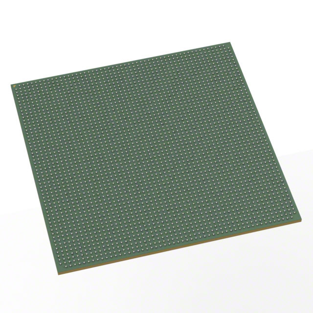
Stratix® 10 DX Field Programmable Gate Array (FPGA) IC 816 240123904 2753000 2912-BBGA, FCBGA |
|---|---|
| Quantity | 694 Available (as of October 7, 2026) |

| Product Category | Field Programmable Gate Array (FPGA) |
|---|---|
| Manufacturer | Intel |
| Manufacturing Status | Obsolete |
| Manufacturer Standard Lead Time | Contact Us |
| Datasheet |
Specifications & Environmental
| Device Package | 2912-FBGA (55x55) | Grade | Extended | Operating Temperature | 0°C – 100°C | ||
|---|---|---|---|---|---|---|---|
| Package / Case | 2912-BBGA, FCBGA | Number of I/O | 816 | Voltage | 870 mV - 970 mV | ||
| Mounting Method | Surface Mount | RoHS Compliance | Unknown | REACH Compliance | REACH Unknown | ||
| Moisture Sensitivity Level | 3 (168 Hours) | Number of LABs/CLBs | N/A | Number of Logic Elements/Cells | 2753000 | ||
| Number of Gates | N/A | ECCN | OBSOLETE | HTS Code | N/A | ||
| Qualification | N/A | Total RAM Bits | 240123904 |
Overview of 1SD280PT2F55E2VGS1 – Stratix® 10 DX FPGA, 2,753,000 logic elements
The 1SD280PT2F55E2VGS1 is an Intel Stratix® 10 DX field-programmable gate array (FPGA) supplied in a 2912-BBGA flip-chip package. It combines a high-capacity programmable fabric with Stratix 10 DX family features such as the Intel Hyperflex core architecture and a range of integrated hard intellectual-property blocks for compute and high-bandwidth I/O.
Designed for high-performance acceleration in markets such as datacenter, networking, cloud computing and test & measurement, this device delivers large logic and memory resources, extensive I/O, and advanced transceiver and interface capabilities suitable for demanding system designs.
Key Features
- Core & Architecture Intel Stratix 10 DX family architecture with Intel Hyperflex core technology as described for the Stratix 10 DX device series.
- Logic Capacity 2,753,000 logic elements (cells) for implementing large, complex designs.
- Internal Memory 240,123,904 total RAM bits providing significant on-chip storage for buffers, FIFOs and design state.
- I/O Density 816 user I/O pins to support broad connectivity and multiple external interfaces.
- High-Speed Transceivers & Hard IP Stratix 10 DX family devices include heterogeneous transceiver tiles and hard IP for protocols such as PCIe Gen4 and 100 GbE; the family supports high-speed serial signaling for demanding link applications.
- Memory & External Interfaces Series features include DDR4 memory controllers and a DDR‑T soft IP controller option for attaching persistent memory; select devices in the family may include HBM2 stacked DRAM.
- Package & Mounting 2912-BBGA (2912-FBGA 55×55) flip-chip BGA, surface-mount mounting type for high-density board designs.
- Power & Supply Specified core voltage supply range of 870 mV to 970 mV.
- Temperature & Grade Extended grade with an operating temperature range of 0 °C to 100 °C.
- Compliance RoHS compliant.
Typical Applications
- Datacenter Acceleration Hardware acceleration, protocol offload and custom compute kernels where large logic capacity and high-bandwidth I/O reduce latency and increase throughput.
- High-Speed Networking Packet processing, line-rate encryption/decryption, and networking appliances leveraging integrated hard IP for 100 GbE and high-speed transceivers.
- Cloud & Infrastructure Compute and I/O aggregation functions, including PCIe Gen4 connectivity for high-throughput host interfaces.
- Test & Measurement Real-time signal processing and capture systems that require extensive on-chip memory and large programmable logic resources.
Unique Advantages
- Large, Scalable Logic Resource: 2,753,000 logic elements enable complex implementions without partitioning across multiple devices.
- Substantial On-Chip Memory: 240,123,904 bits of RAM provide capacity for buffering, packet storage and algorithm state close to the logic fabric.
- Extensive I/O Count: 816 I/Os allow flexible interfacing to a wide range of peripherals, memory, and module connectors.
- Family-Level High-Speed Interfaces: Stratix 10 DX family hard IP for PCIe Gen4, 100 GbE, and advanced transceiver technology simplifies integration of high-bandwidth links.
- Advanced Packaging: 2912-BBGA flip-chip package (55×55) supports dense routing and thermal performance for high-pin-count designs.
- Documented Platform: Features and architecture details are provided in the Stratix 10 DX device documentation to support design planning and integration.
Why Choose 1SD280PT2F55E2VGS1?
The 1SD280PT2F55E2VGS1 positions itself as a high-capacity Stratix 10 DX family FPGA for system designs that require extensive programmable logic, large on-chip memory, and significant I/O resources. Its specification set — including 2,753,000 logic elements, 240,123,904 RAM bits, and 816 I/Os — supports complex algorithms, large data buffering and multi-protocol interfacing within a single device.
This device is suitable for engineering teams developing datacenter acceleration, high-speed networking, cloud infrastructure, and test & measurement equipment who need a scalable, well-documented FPGA platform with family-level connectivity and high-speed interface options. The extended-grade temperature range and RoHS compliance make it appropriate for many demanding commercial deployments.
Request a quote or contact sales to discuss pricing, availability and how the 1SD280PT2F55E2VGS1 can fit into your next high-performance FPGA design.
























Date Founded: 1968
Headquarters: Santa Clara, California, USA
Employees: 130,000+
Revenue: $54.23 Billion
Certifications and Memberships: ISO9001:2015, ISO14001:2015, ISO17025:2017, ISO27001:2022, ISO45001:2018, ISO50001:2018


