
1SD280PT2F55I1VGS1
| Part Description |
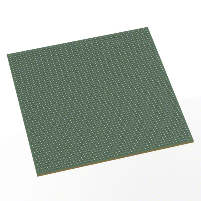
Stratix® 10 DX Field Programmable Gate Array (FPGA) IC 816 240123904 2753000 2912-BBGA, FCBGA |
|---|---|
| Quantity | 397 Available (as of June 15, 2026) |

| Product Category | Field Programmable Gate Array (FPGA) |
|---|---|
| Manufacturer | Intel |
| Manufacturing Status | Obsolete |
| Manufacturer Standard Lead Time | Contact Us |
| Datasheet |
Specifications & Environmental
| Device Package | 2912-FBGA (55x55) | Grade | Industrial | Operating Temperature | -40°C – 100°C | ||
|---|---|---|---|---|---|---|---|
| Package / Case | 2912-BBGA, FCBGA | Number of I/O | 816 | Voltage | 870 mV - 970 mV | ||
| Mounting Method | Surface Mount | RoHS Compliance | Unknown | REACH Compliance | REACH Unknown | ||
| Moisture Sensitivity Level | 3 (168 Hours) | Number of LABs/CLBs | N/A | Number of Logic Elements/Cells | 2753000 | ||
| Number of Gates | N/A | ECCN | OBSOLETE | HTS Code | N/A | ||
| Qualification | N/A | Total RAM Bits | 240123904 |
Overview of 1SD280PT2F55I1VGS1 – Stratix® 10 DX Field Programmable Gate Array (FPGA) IC
The 1SD280PT2F55I1VGS1 is an Intel Stratix® 10 DX FPGA provided in a 2912-BBGA FCBGA package (supplier package: 2912-FBGA, 55×55). It delivers a high-density, industrial-grade programmable fabric tailored for compute- and I/O-intensive designs.
Built on the Stratix 10 DX family architecture, this device targets datacenter, networking, cloud computing and test & measurement applications by combining large logic capacity, extensive on-chip RAM, and high-speed transceiver and protocol support described for the DX series.
Key Features
- Logic Capacity Provides 2,753,000 logic element cells for complex programmable logic and custom acceleration tasks.
- On-Chip Memory Includes 240,123,904 total RAM bits to support large buffering, on-chip data structures, and high-throughput pipelines.
- I/O Density Offers 816 user I/O pins to support wide external interfacing and high port counts in compact board designs.
- Stratix 10 DX Architecture Part of the Stratix 10 DX family which features the Intel Hyperflex core architecture, variable precision DSP blocks, and family-level hard IP such as PCIe Gen4 and 100 GbE (as described in the Stratix 10 DX overview).
- High-Speed Transceivers (family-level) The Stratix 10 DX family documentation indicates heterogeneous transceiver tiles supporting up to 57.8 Gbps PAM4 and 28.9 Gbps NRZ signaling for high-bandwidth serial links.
- Memory & IP Integration (family-level) DX-series devices support advanced memory and IP options including HBM2 and hard DDR4/PCIe IP blocks, plus DDR-T soft IP for direct attachment of persistent memory modules (per family datasheet).
- Package & Mounting Surface-mount device in a 2912-BBGA FCBGA package; supplier package listed as 2912-FBGA (55×55).
- Supply & Temperature Specified core supply range 870 mV to 970 mV and industrial operating temperature range of −40 °C to 100 °C.
- Compliance RoHS compliant.
Typical Applications
- Datacenter Acceleration Use for compute acceleration and custom offload engines where high logic density and on-chip memory accelerate data-path processing.
- High‑Performance Networking Deploy in switches, routers, and line cards that require large I/O counts and support for high-speed serial transceivers and hardened protocol IP (as provided by the Stratix 10 DX family).
- Cloud & Storage Interfaces Implement controllers and protocol bridges that leverage the device’s memory capacity and family-level PCIe/DDR IP to connect to high-throughput storage and persistent memory subsystems.
- Test & Measurement Systems Integrate into instrumentation that demands deterministic logic, large on-chip RAM for capture/analysis, and wide external I/O.
Unique Advantages
- High Logic Density: 2,753,000 logic element cells enable complex, high-parallelism designs without immediate partitioning across multiple FPGAs.
- Substantial On-Chip Memory: 240,123,904 total RAM bits reduce dependence on external memory for buffering and real-time data processing.
- Extensive I/O Capability: 816 I/O pins support broad peripheral and high-port-count interfaces directly at the device edge.
- Industrial Temperature Rating: Operates from −40 °C to 100 °C, supporting deployed systems with extended ambient and thermal ranges.
- Advanced Family-Level Integration: As a Stratix 10 DX device, it benefits from family-level architectural elements such as Hyperflex cores, variable-precision DSPs, EMIB packaging technology, and hardened protocol IP to simplify system-level integration.
- Compact High-Pin Package: 2912-BBGA FCBGA (2912-FBGA, 55×55) balances high I/O and logic capacity in a single package for space-constrained boards.
Why Choose 1SD280PT2F55I1VGS1?
The 1SD280PT2F55I1VGS1 combines large logic capacity, significant on-chip memory, and high I/O density in an industrial-grade Stratix 10 DX FPGA package. It is positioned for engineers building data‑plane acceleration, high-performance networking, and measurement systems that demand programmable throughput and platform-level integration described by the Stratix 10 DX family.
Choosing this device provides a path to scalable, high-bandwidth designs with family-level capabilities—such as hardened protocol IP and advanced packaging technologies—backed by documented Stratix 10 DX architecture features. The part is suited to teams that require a dense programmable fabric with robust thermal and supply specifications for deployed systems.
Request a quote or submit an inquiry for pricing and availability to move your design forward with 1SD280PT2F55I1VGS1.


Date Founded: 1968
Headquarters: Santa Clara, California, USA
Employees: 130,000+
Revenue: $54.23 Billion
Certifications and Memberships: ISO9001:2015, ISO14001:2015, ISO17025:2017, ISO27001:2022, ISO45001:2018, ISO50001:2018


