
5AGXBA1D4F27C4G
| Part Description |
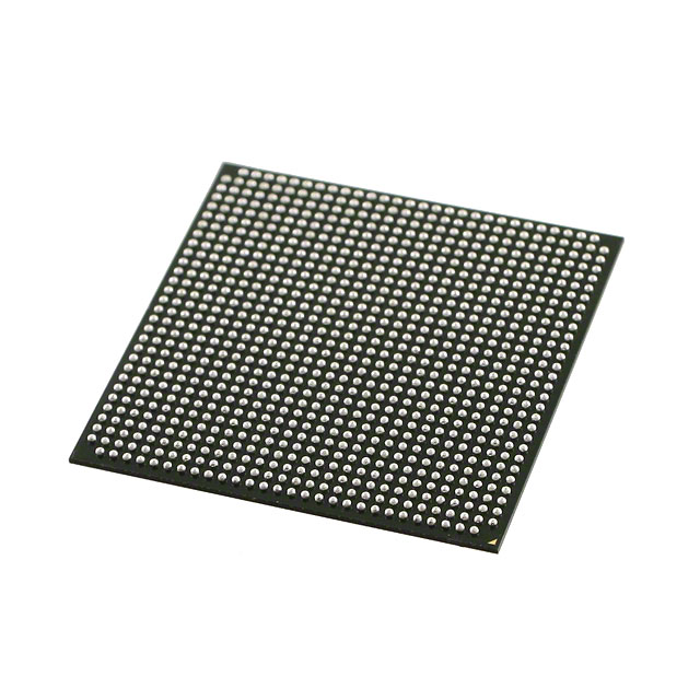
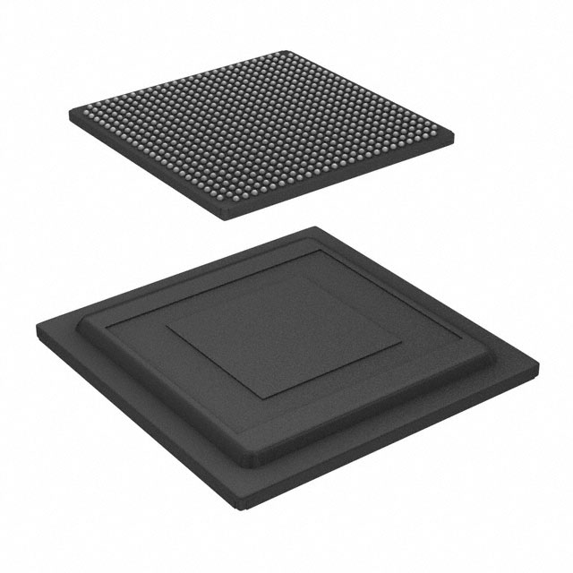
Arria V GX Field Programmable Gate Array (FPGA) IC 336 8666112 75000 672-BBGA, FCBGA |
|---|---|
| Quantity | 1,423 Available (as of October 8, 2026) |

| Product Category | Field Programmable Gate Array (FPGA) |
|---|---|
| Manufacturer | Intel |
| Manufacturing Status | Active |
| Manufacturer Standard Lead Time | 16 Weeks |
| Datasheet |
Specifications & Environmental
| Device Package | 672-FBGA (27x27) | Grade | Commercial | Operating Temperature | 0°C – 85°C | ||
|---|---|---|---|---|---|---|---|
| Package / Case | 672-BBGA, FCBGA | Number of I/O | 336 | Voltage | 1.07 V - 1.13 V | ||
| Mounting Method | Surface Mount | RoHS Compliance | RoHS Compliant | REACH Compliance | REACH Unaffected | ||
| Moisture Sensitivity Level | 3 (168 Hours) | Number of LABs/CLBs | 3537 | Number of Logic Elements/Cells | 75000 | ||
| Number of Gates | N/A | ECCN | PENDING ECCN | HTS Code | 0000.00.0000 | ||
| Qualification | N/A | Total RAM Bits | 8666112 |
Overview of 5AGXBA1D4F27C4G – Arria V GX FPGA, 75,000 logic elements, 672‑BBGA
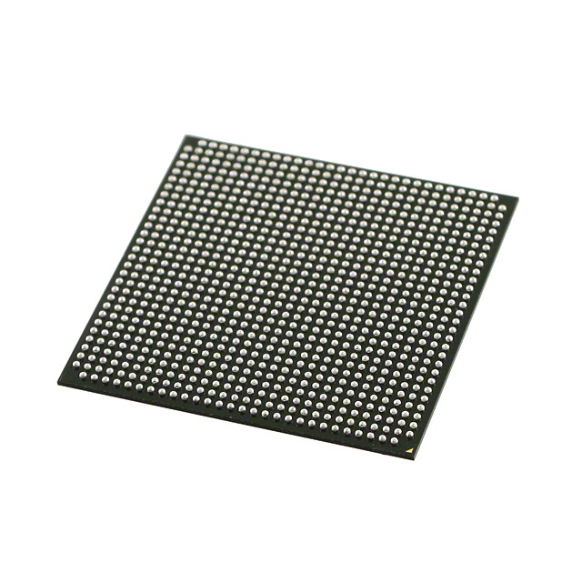
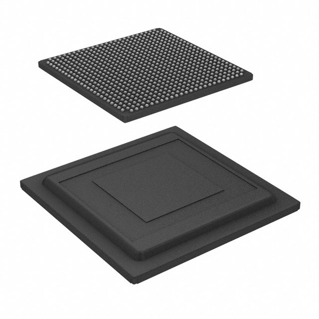
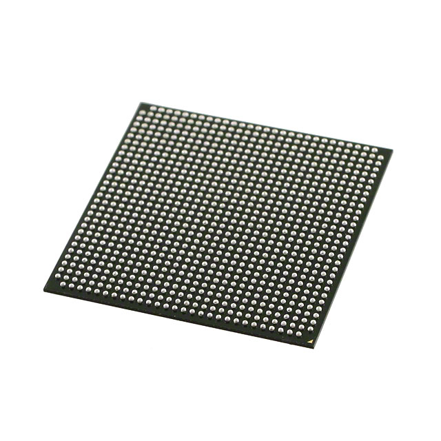
The 5AGXBA1D4F27C4G is an Arria V GX field programmable gate array (FPGA) in a 672‑ball BGA (FCBGA) package designed for surface‑mount PCB assembly. It delivers a high logic element count and substantial on‑chip RAM in a compact 27×27 672‑FBGA footprint for commercial‑grade embedded designs.
With 75,000 logic elements, 8,666,112 total RAM bits and 336 user I/O, this device targets applications that require dense programmable logic, significant local memory, and a wide I/O complement while operating within a 1.07 V to 1.13 V core supply range and a 0 °C to 85 °C operating window.
Key Features
- Programmable Logic Capacity — 75,000 logic elements to implement complex, custom digital functions and control logic.
- On‑Chip Memory — 8,666,112 total RAM bits for buffering, lookup tables, and state storage close to logic.
- I/O Count — 336 user I/O pins to support rich peripheral and device interfacing.
- Package and Mounting — 672‑BBGA (supplier package: 672‑FBGA, 27×27) in a surface‑mount FCBGA package for high‑density PCB layouts.
- Power Supply — Core supply range of 1.07 V to 1.13 V to match system power domains and regulator designs.
- Commercial Grade — Rated for commercial applications with an operating temperature range of 0 °C to 85 °C.
- Regulatory — RoHS compliant for lead‑free assembly and environmental regulatory requirements.
Typical Applications
- Custom digital processing and prototyping — Use the 75,000 logic elements and multi‑megabit on‑chip RAM to implement bespoke logic, control engines, and prototype systems on a single device.
- High‑density I/O interfacing — 336 user I/O pins enable consolidation of multiple peripheral interfaces and front‑end connectivity onto the FPGA.
- Embedded acceleration and offload — Local RAM and programmable fabric support deterministic hardware acceleration for compute‑intensive tasks within commercial systems.
Unique Advantages
- High logic density: 75,000 logic elements provide the capacity to integrate large state machines, custom accelerators, and control logic without external ASICs.
- Substantial on‑chip RAM: 8,666,112 total RAM bits reduce reliance on external memory for buffering and temporary data storage, simplifying board design.
- Ample I/O resources: 336 I/O pins allow flexible interfacing to sensors, peripherals, and transceivers, enabling system consolidation.
- Compact BGA footprint: 672‑FBGA (27×27) package balances high pin count with a space‑efficient footprint for dense PCB implementations.
- Commercial temperature and RoHS compliance: Designed for commercial deployments and lead‑free manufacturing processes.
Why Choose 5AGXBA1D4F27C4G?
The 5AGXBA1D4F27C4G Arria V GX FPGA combines substantial programmable logic, multi‑megabit on‑chip RAM, and a wide I/O complement in a compact 672‑ball FCBGA package, making it well suited for commercial embedded designs that require integrated, reconfigurable logic and memory. Its defined core voltage range and commercial temperature rating make it straightforward to integrate into standard power and thermal designs.
This device is appropriate for engineering teams looking to consolidate logic, reduce external components, and accelerate time‑to‑market with a programmable solution backed by the Arria V device family documentation.
Request a quote or submit a purchasing inquiry to receive availability, pricing, and lead‑time information for the 5AGXBA1D4F27C4G Arria V GX FPGA.




















Date Founded: 1968
Headquarters: Santa Clara, California, USA
Employees: 130,000+
Revenue: $54.23 Billion
Certifications and Memberships: ISO9001:2015, ISO14001:2015, ISO17025:2017, ISO27001:2022, ISO45001:2018, ISO50001:2018


