
5AGXBB1D4F31C5N
| Part Description |
Arria V GX Field Programmable Gate Array (FPGA) IC 384 17358848 300000 896-BBGA, FCBGA |
|---|---|
| Quantity | 241 Available (as of June 15, 2026) |

| Product Category | Field Programmable Gate Array (FPGA) |
|---|---|
| Manufacturer | Intel |
| Manufacturing Status | Obsolete |
| Manufacturer Standard Lead Time | Contact Us |
| Datasheet |
Specifications & Environmental
| Device Package | 896-FBGA (31x31) | Grade | Commercial | Operating Temperature | 0°C – 85°C | ||
|---|---|---|---|---|---|---|---|
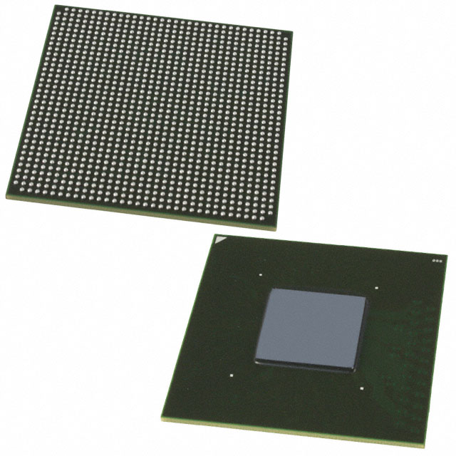
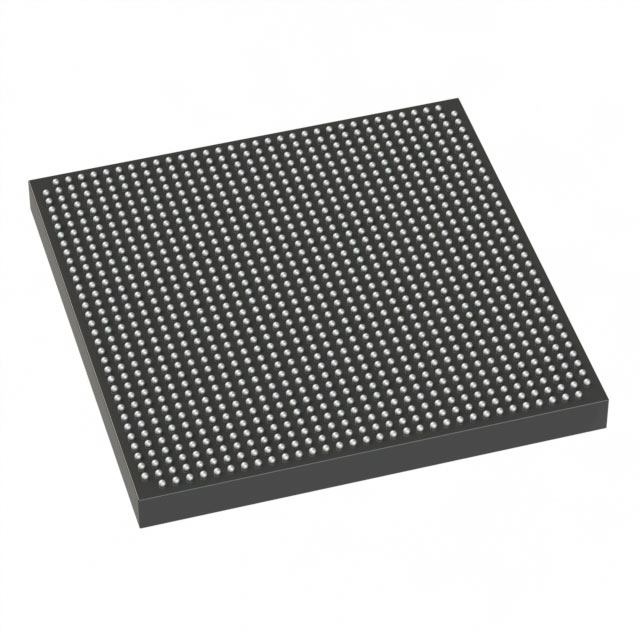
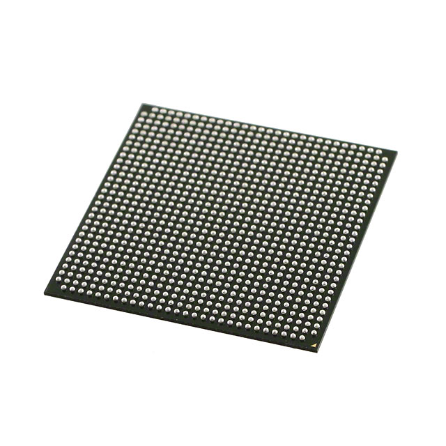
| Package / Case | 896-BBGA, FCBGA | Number of I/O | 384 | Voltage | 1.07 V - 1.13 V | ||
| Mounting Method | Surface Mount | RoHS Compliance | RoHS Compliant | REACH Compliance | REACH Unknown | ||
| Moisture Sensitivity Level | 3 (168 Hours) | Number of LABs/CLBs | 14151 | Number of Logic Elements/Cells | 300000 | ||
| Number of Gates | N/A | ECCN | 3A001A2C | HTS Code | 8542.39.0001 | ||
| Qualification | N/A | Total RAM Bits | 17358848 |
Overview of 5AGXBB1D4F31C5N – Arria V GX FPGA, 300,000 logic elements
The 5AGXBB1D4F31C5N is an Arria V GX field-programmable gate array (FPGA) in a high-density 896-ball BGA (FCBGA) package. It provides 300,000 logic elements and approximately 17.36 Mbits of embedded memory, with up to 384 general-purpose I/Os—delivering a platform for designs that require substantial programmable logic, on-chip RAM, and broad I/O integration.
Offered as a commercial-grade device with a documented operating voltage range of 1.07 V to 1.13 V and an ambient operating temperature range of 0 °C to 85 °C, this device is suited to commercial embedded and system-level applications where dense logic and memory resources are required.
Key Features
- Core Logic 300,000 logic elements to implement large-scale programmable logic functions and complex custom logic blocks.
- Embedded Memory Approximately 17.36 Mbits of on-chip RAM for buffers, FIFOs, and scratchpad storage close to logic.
- I/O Capacity Up to 384 I/O pins to support wide parallel interfaces, multiple peripherals, and system-level connectivity.
- Power and Supply Specified core supply voltage from 1.07 V to 1.13 V for predictable power budgeting and core operation.
- Package and Mounting 896-BBGA FCBGA package (supplier device package: 896-FBGA, 31×31) designed for surface-mount assembly.
- Operating Grade and Temperature Commercial grade with an operating temperature range of 0 °C to 85 °C.
- Compliance RoHS-compliant for alignment with common environmental requirements.
Typical Applications
- High-density programmable systems Implements large custom logic functions and datapaths using 300,000 logic elements and substantial embedded RAM.
- Multi-channel I/O platforms Supports designs requiring broad parallel connectivity or numerous external interfaces with up to 384 I/Os.
- Embedded compute and buffering On-chip memory (approximately 17.36 Mbits) for local buffering, streaming, and storage closely coupled to logic.
Unique Advantages
- High logic capacity: 300,000 logic elements enable implementation of complex control, signal processing, and custom acceleration functions without immediate need for external logic.
- Substantial on-chip memory: Approximately 17.36 Mbits of embedded RAM reduces dependence on external memory for intermediate storage and buffering.
- Large I/O complement: 384 I/Os simplify system integration by accommodating multiple interfaces and parallel signals directly at the FPGA.
- Compact surface-mount package: 896-ball FCBGA (31×31) balances high pin count with a board-level form factor suitable for surface-mount assembly.
- Commercial operating range: Documented 0 °C to 85 °C temperature rating and defined core supply range (1.07 V–1.13 V) support predictable design and validation in commercial deployments.
- RoHS compliant: Aligns with common environmental regulations for electronic assemblies.
Why Choose 5AGXBB1D4F31C5N?
The 5AGXBB1D4F31C5N Arria V GX FPGA combines a high logic count, significant embedded RAM, and extensive I/O in a single commercial-grade FCBGA package. It is positioned for designers who need dense programmable logic and integrated memory resources with a clearly defined supply and thermal envelope.
This device is appropriate for development teams building complex embedded systems, high-channel I/O designs, or applications where consolidating logic and memory into a single device reduces board-level complexity. Documentation for the Arria V family provides the electrical and configuration specifications required for system integration and validation.
Request a quote or submit a purchase inquiry to get pricing and availability for the 5AGXBB1D4F31C5N Arria V GX FPGA.


Date Founded: 1968
Headquarters: Santa Clara, California, USA
Employees: 130,000+
Revenue: $54.23 Billion
Certifications and Memberships: ISO9001:2015, ISO14001:2015, ISO17025:2017, ISO27001:2022, ISO45001:2018, ISO50001:2018


