
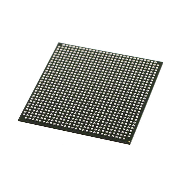
5AGXBB1D4F31C5G
| Part Description |
Arria V GX Field Programmable Gate Array (FPGA) IC 384 17358848 300000 896-BBGA, FCBGA |
|---|---|
| Quantity | 1,976 Available (as of October 7, 2026) |
| Product Category | Field Programmable Gate Array (FPGA) |
|---|---|
| Manufacturer | Intel |
| Manufacturing Status | Active |
| Manufacturer Standard Lead Time | 12 Weeks |
| Datasheet |
Specifications & Environmental
| Device Package | 896-FBGA (31x31) | Grade | Commercial | Operating Temperature | 0°C – 85°C | ||
|---|---|---|---|---|---|---|---|
| Package / Case | 896-BBGA, FCBGA | Number of I/O | 384 | Voltage | 1.07 V - 1.13 V | ||
| Mounting Method | Surface Mount | RoHS Compliance | RoHS Compliant | REACH Compliance | REACH Unaffected | ||
| Moisture Sensitivity Level | 3 (168 Hours) | Number of LABs/CLBs | 14151 | Number of Logic Elements/Cells | 300000 | ||
| Number of Gates | N/A | ECCN | PENDING ECCN | HTS Code | 0000.00.0000 | ||
| Qualification | N/A | Total RAM Bits | 17358848 |
Overview of 5AGXBB1D4F31C5G – Arria V GX Field Programmable Gate Array (FPGA), 300,000 logic elements
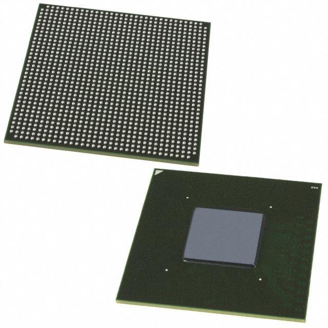
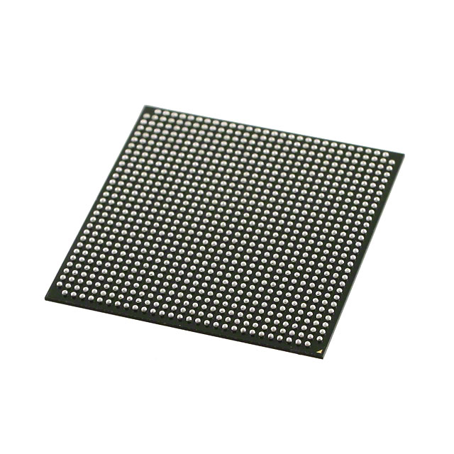
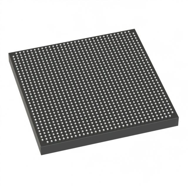
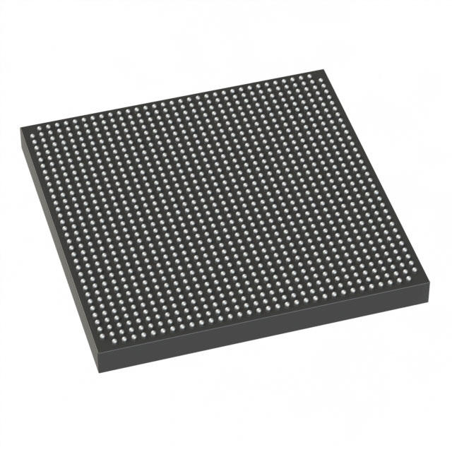
The 5AGXBB1D4F31C5G is an Intel Arria V GX field programmable gate array (FPGA) supplied in an 896‑ball FCBGA package. It provides a high-density logic fabric with substantial on-chip RAM and a large I/O count, making it suitable for designs that require significant programmable logic and memory resources within a compact BGA footprint.
Key attributes include 300,000 logic elements, 17,358,848 total RAM bits, 384 user I/O, a core supply range of 1.07–1.13 V, and commercial operating temperature support (0 °C to 85 °C). The device is RoHS compliant.
Key Features
- Logic Capacity — 300,000 logic elements provide substantial programmable logic resources for complex digital designs and custom processing blocks.
- On‑Chip Memory — 17,358,848 total RAM bits enable large buffers, FIFOs, and local data storage without external memory for many functions.
- I/O Resources — 384 user I/O pins support rich peripheral connectivity and multi‑channel interfaces.
- Package — 896‑FBGA (31 × 31) FCBGA package offers a high‑density SMT footprint for space‑constrained boards.
- Power — Core voltage supply range of 1.07 V to 1.13 V allows precise power planning for core domains.
- Operating Grade — Commercial grade operation across 0 °C to 85 °C for standard embedded and industrial‑environment electronics.
- Regulatory — RoHS compliant.
Typical Applications
- FPGA‑based prototyping and system integration — High logic capacity and on‑chip RAM support complex prototype designs and integration of custom IP blocks.
- Compute acceleration — Large logic and memory resources enable implementation of hardware accelerators and parallel processing engines.
- High‑density I/O systems — 384 I/O pins accommodate multi‑channel interfaces, front‑end aggregation, and extensive peripheral connectivity.
Unique Advantages
- Large programmable fabric — 300,000 logic elements allow integration of sizeable custom logic and multiple IP cores on a single device.
- Substantial on‑chip memory — 17,358,848 RAM bits reduce dependence on external memory for many buffering and local storage needs.
- Extensive I/O capacity — 384 user I/O simplify routing of numerous interfaces without additional multiplexing logic.
- Compact, high‑density packaging — 896‑FBGA (31×31) FCBGA provides high pin count in a space‑efficient surface‑mount form factor.
- Predictable power domain — Narrow core voltage range (1.07–1.13 V) supports defined power budgeting and supply design.
- Commercial grade reliability — Rated for 0 °C to 85 °C operation and RoHS compliant for standard commercial deployments.
Why Choose 5AGXBB1D4F31C5G?
The 5AGXBB1D4F31C5G Arria V GX FPGA balances high logic density, extensive on‑chip RAM, and abundant I/O in a single 896‑FBGA package. Its specification set is targeted at designers who need a compact FPGA platform capable of hosting large custom logic, substantial local memory, and numerous interfaces while operating within standard commercial temperature ranges.
This device is well suited to teams building complex digital systems that require consolidation of logic and memory resources to reduce board-level complexity and accelerate development cycles. The combination of specified electrical, memory, and I/O resources offers clear, verifiable parameters for system architects and procurement.
Request a quote or submit a procurement inquiry to obtain pricing, availability, and ordering information for the 5AGXBB1D4F31C5G Arria V GX FPGA.





















Date Founded: 1968
Headquarters: Santa Clara, California, USA
Employees: 130,000+
Revenue: $54.23 Billion
Certifications and Memberships: ISO9001:2015, ISO14001:2015, ISO17025:2017, ISO27001:2022, ISO45001:2018, ISO50001:2018


