
5AGXBB1D4F31I5N
| Part Description |
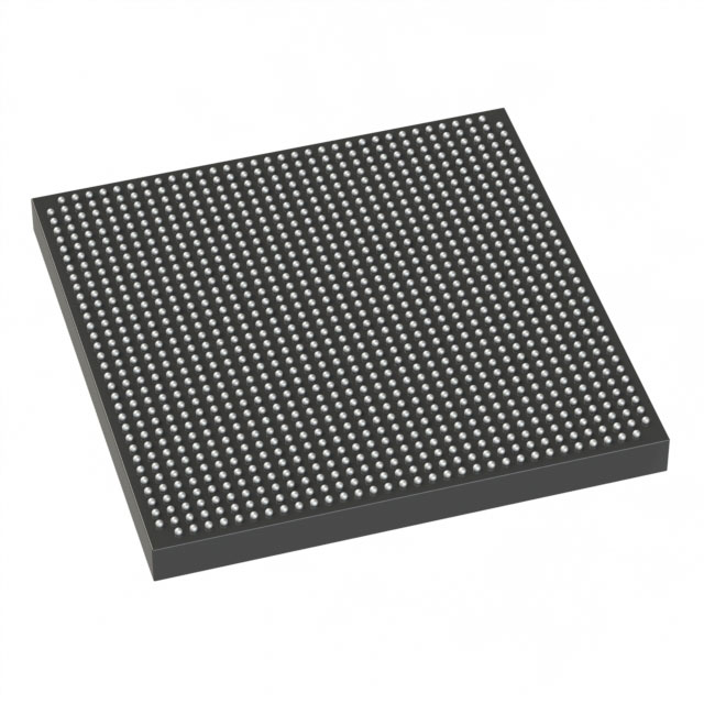
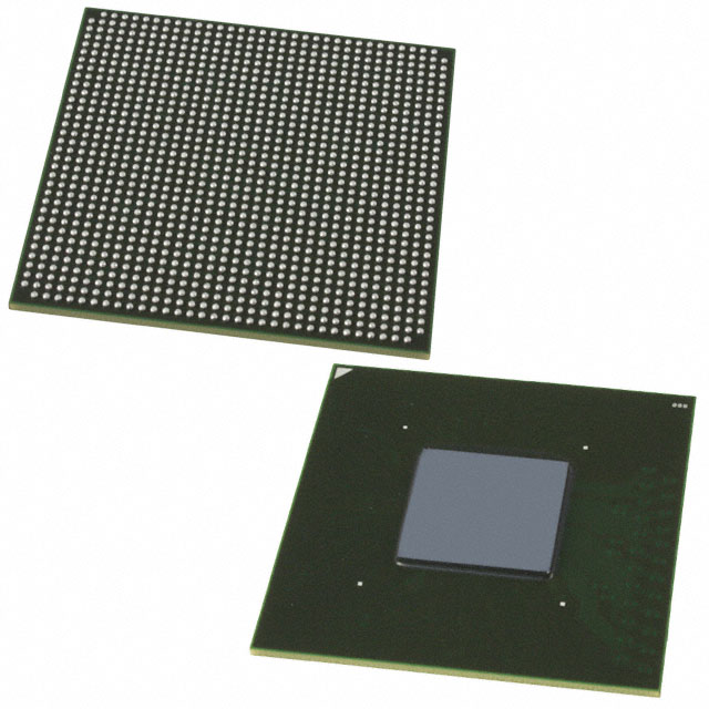
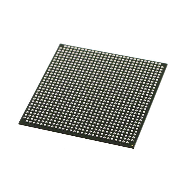
Arria V GX Field Programmable Gate Array (FPGA) IC 384 17358848 300000 896-BBGA, FCBGA |
|---|---|
| Quantity | 19 Available (as of June 10, 2026) |

| Product Category | Field Programmable Gate Array (FPGA) |
|---|---|
| Manufacturer | Intel |
| Manufacturing Status | Obsolete |
| Manufacturer Standard Lead Time | Contact Us |
| Datasheet |
Specifications & Environmental
| Device Package | 896-FBGA (31x31) | Grade | Industrial | Operating Temperature | -40°C – 100°C | ||
|---|---|---|---|---|---|---|---|
| Package / Case | 896-BBGA, FCBGA | Number of I/O | 384 | Voltage | 1.07 V - 1.13 V | ||
| Mounting Method | Surface Mount | RoHS Compliance | RoHS Compliant | REACH Compliance | REACH Unknown | ||
| Moisture Sensitivity Level | 3 (168 Hours) | Number of LABs/CLBs | 14151 | Number of Logic Elements/Cells | 300000 | ||
| Number of Gates | N/A | ECCN | 3A001A2C | HTS Code | 8542.39.0001 | ||
| Qualification | N/A | Total RAM Bits | 17358848 |
Overview of 5AGXBB1D4F31I5N – Arria V GX FPGA, 300,000 Logic Elements, 384 I/Os
The 5AGXBB1D4F31I5N is an Arria V GX Field Programmable Gate Array (FPGA) in an 896-BBGA FCBGA package. The device provides a high-density programmable fabric with approximately 300,000 logic elements and substantial on-chip memory to support complex, customizable digital designs. Its industrial-grade rating and wide operating temperature range make it suitable for designs that require reliable operation across extended temperature conditions.
Key Features
- Core Logic Density Approximately 300,000 logic elements for implementing large-scale custom logic and hardware acceleration.
- Embedded Memory Approximately 17.36 Mbits of total on-chip RAM available for buffering, FIFOs, and on-chip data storage.
- I/O Capacity 384 user I/Os to support wide parallel interfaces, multiple peripherals, and board-level connectivity.
- Industrial Grade and Temperature Range Industrial-grade device specified for operation from −40 °C to 100 °C, enabling deployment in temperature-challenging environments.
- Power and Voltage Core voltage supplied in the range 1.07 V to 1.13 V, enabling predictable power sequencing and design planning.
- Package and Mounting 896-BBGA (FCBGA) package; supplier device package listed as 896-FBGA (31×31). Surface-mount device suitable for modern PCB assembly.
- Standards Compliance RoHS compliant, supporting regulatory and environmental requirements.
- Comprehensive Datasheet Coverage Datasheet sections include electrical characteristics, switching characteristics, configuration specifications, and I/O timing for detailed electrical and timing design reference.
Typical Applications
- Communications & Networking High logic density and large I/O count support packet processing, custom protocol implementations, and interface bridging.
- Embedded Acceleration On-chip RAM and extensive logic enable custom hardware acceleration and data-path implementations for compute-intensive tasks.
- Industrial Control Industrial-grade temperature rating and robust I/O make the device suitable for factory automation, motor control logic, and machine control systems.
- High-Density Interface Conversion Large I/O complement and programmable fabric allow consolidating multiple interface functions into a single device to reduce system complexity.
Unique Advantages
- High logic capacity: Enables consolidation of complex functions and multiple IP blocks into one FPGA, reducing bill of materials and board-level complexity.
- Significant embedded memory: Approximately 17.36 Mbits of on-chip RAM supports deep buffering, packet queues, and stateful algorithms without relying solely on external memory.
- Large I/O complement: 384 I/Os provide flexibility for high-pin-count interfaces, parallel buses, and multiple peripheral connections.
- Industrial temperature operation: Rated for −40 °C to 100 °C, the device helps deliver reliable performance in demanding environmental conditions.
- Surface-mount, compact package: 896-BBGA (31×31) FCBGA package balances high pin-count capability with a compact board footprint for dense system designs.
- RoHS compliant: Aligns with environmental regulations and eases compliance in product development and manufacturing.
Why Choose 5AGXBB1D4F31I5N?
The 5AGXBB1D4F31I5N Arria V GX FPGA delivers a combination of high logic density, substantial on-chip RAM, and a broad I/O complement in an industrial-grade, surface-mount package. These characteristics make it well-suited for designers building complex, high-throughput digital systems that require customizable hardware, robust I/O, and reliable operation across extended temperature ranges.
Designed for applications that demand significant programmable resources and system integration, this device supports scalable designs and long-term deployment with clear electrical and timing documentation provided in the device datasheet.
Request a quote or submit an inquiry to receive pricing, availability, and lead-time information for the 5AGXBB1D4F31I5N Arria V GX FPGA.


Date Founded: 1968
Headquarters: Santa Clara, California, USA
Employees: 130,000+
Revenue: $54.23 Billion
Certifications and Memberships: ISO9001:2015, ISO14001:2015, ISO17025:2017, ISO27001:2022, ISO45001:2018, ISO50001:2018


