
5AGXBB1D4F35C4G
| Part Description |
Arria V GX Field Programmable Gate Array (FPGA) IC 544 17358848 300000 1152-BBGA, FCBGA |
|---|---|
| Quantity | 1,869 Available (as of June 10, 2026) |

| Product Category | Field Programmable Gate Array (FPGA) |
|---|---|
| Manufacturer | Intel |
| Manufacturing Status | Active |
| Manufacturer Standard Lead Time | 12 Weeks |
| Datasheet |
Specifications & Environmental
| Device Package | 1152-FBGA, FC (35x35) | Grade | Commercial | Operating Temperature | 0°C – 85°C | ||
|---|---|---|---|---|---|---|---|
| Package / Case | 1152-BBGA, FCBGA | Number of I/O | 544 | Voltage | 1.07 V - 1.13 V | ||
| Mounting Method | Surface Mount | RoHS Compliance | RoHS Compliant | REACH Compliance | REACH Unaffected | ||
| Moisture Sensitivity Level | 3 (168 Hours) | Number of LABs/CLBs | 14151 | Number of Logic Elements/Cells | 300000 | ||
| Number of Gates | N/A | ECCN | PENDING ECCN | HTS Code | 0000.00.0000 | ||
| Qualification | N/A | Total RAM Bits | 17358848 |
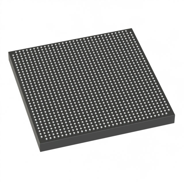
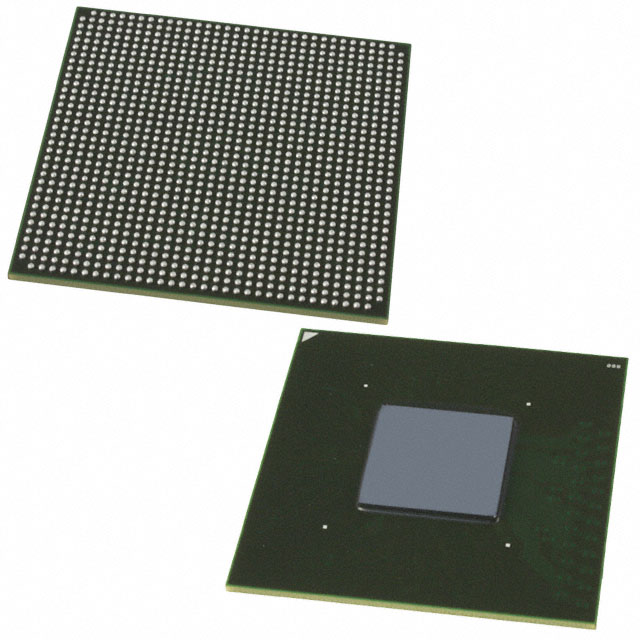
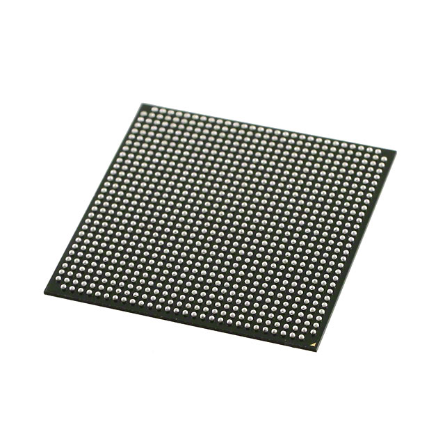
Overview of 5AGXBB1D4F35C4G – Arria V GX FPGA, 300000 logic elements, 1152-BBGA
The 5AGXBB1D4F35C4G is an Arria V GX Field Programmable Gate Array (FPGA) in a 1152-ball FCBGA package designed for high-density programmable logic implementations. This commercial-grade device integrates 300,000 logic elements, a large block RAM resource, and extensive I/O count to support complex, I/O-rich designs that require substantial on-chip resources and tight board-level integration.
Key Features
- High-density logic: 300,000 logic elements provide substantial programmable logic capacity for complex digital designs.
- Embedded memory: Approximately 17.36 Mbits of total on-chip RAM bits (17,358,848 bits) to support buffering, lookup tables, and data storage inside the device.
- Extensive I/O: 544 user I/O pins to enable connectivity to a wide range of external peripherals and interfaces.
- Package and mounting: 1152-BBGA FCBGA package (supplier device package: 1152-FBGA, FC (35×35)) for dense board-level integration and surface-mount assembly.
- Power supply range: Core supply range specified at 1.07 V to 1.13 V for predictable power design and regulation.
- Commercial grade temperature: Rated operating temperature from 0 °C to 85 °C for standard commercial applications.
- Standards compliance: RoHS compliant to meet environmental and manufacturing requirements.
Typical Applications
- Programmable digital logic: Implement custom logic blocks, state machines, and control functions using the device’s large logic-element and embedded memory resources.
- I/O-intensive systems: Systems that require many external interfaces can utilize the 544 I/O pins for parallel connections, bus interfaces, and multi-channel signaling.
- On-chip data buffering: Leverage approximately 17.36 Mbits of embedded RAM for intermediate buffering, packet storage, or LUT-based functions within the FPGA fabric.
Unique Advantages
- Large programmable fabric: 300,000 logic elements enable implementation of dense logic and wide datapaths without immediate need for multiple devices.
- Substantial on-chip memory: Nearly 17.36 Mbits of RAM reduces external memory dependence and simplifies board-level BOM.
- High pin count: 544 I/Os allow flexible partitioning of front-end interfaces and peripheral connections on a single device.
- Compact package footprint: 1152-ball FCBGA (35×35 mm) provides a balance of density and board space efficiency for high-performance designs.
- Predictable power window: Narrow core voltage specification (1.07–1.13 V) aids in stable power-supply design and system-level power budgeting.
- Commercial availability: Commercial grade (-C speed family options indicated in series documentation) supports mainstream product and prototype development cycles.
Why Choose 5AGXBB1D4F35C4G?
The 5AGXBB1D4F35C4G Arria V GX FPGA combines a high count of logic elements and a large embedded RAM complement with extensive I/O capacity in a compact 1152-ball FCBGA package. Its commercial-grade rating and RoHS compliance make it suitable for mainstream electronic products requiring significant on-chip resources and dense board integration. For projects that demand consolidated programmable logic, on-chip memory, and many external interfaces in a single FPGA, this device offers a clear, specification-driven option backed by Arria V device documentation.
Request a quote or submit a purchasing inquiry to evaluate the 5AGXBB1D4F35C4G for your next design and get component-level details for procurement and system integration.


Date Founded: 1968
Headquarters: Santa Clara, California, USA
Employees: 130,000+
Revenue: $54.23 Billion
Certifications and Memberships: ISO9001:2015, ISO14001:2015, ISO17025:2017, ISO27001:2022, ISO45001:2018, ISO50001:2018


