
5AGXFA7H4F35C5N
| Part Description |
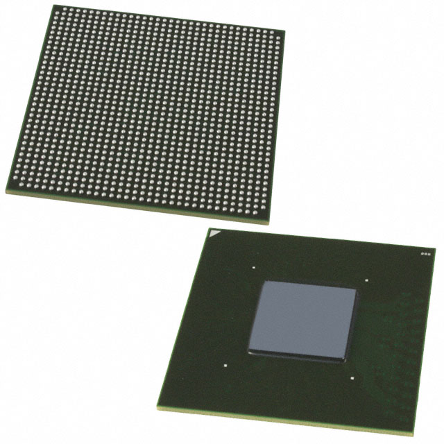
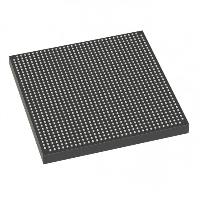
Arria V GX Field Programmable Gate Array (FPGA) IC 544 15470592 242000 1152-BBGA, FCBGA Exposed Pad |
|---|---|
| Quantity | 362 Available (as of June 18, 2026) |

| Product Category | Field Programmable Gate Array (FPGA) |
|---|---|
| Manufacturer | Intel |
| Manufacturing Status | Obsolete |
| Manufacturer Standard Lead Time | Contact Us |
| Datasheet |
Specifications & Environmental
| Device Package | 1152-FBGA (35x35) | Grade | Commercial | Operating Temperature | 0°C – 85°C | ||
|---|---|---|---|---|---|---|---|
| Package / Case | 1152-BBGA, FCBGA Exposed Pad | Number of I/O | 544 | Voltage | 1.07 V - 1.13 V | ||
| Mounting Method | Surface Mount | RoHS Compliance | RoHS Compliant | REACH Compliance | REACH Unknown | ||
| Moisture Sensitivity Level | 3 (168 Hours) | Number of LABs/CLBs | 11460 | Number of Logic Elements/Cells | 242000 | ||
| Number of Gates | N/A | ECCN | 3A001A2C | HTS Code | 8542.39.0001 | ||
| Qualification | N/A | Total RAM Bits | 15470592 |
Overview of 5AGXFA7H4F35C5N – Arria V GX FPGA, 242,000 Logic Elements, 544 I/Os, 1152‑BBGA
The 5AGXFA7H4F35C5N is an Intel Arria V GX field programmable gate array (FPGA) optimized for designs that require high logic capacity and extensive I/O. This device combines substantial on‑chip memory and a large I/O count in a compact FCBGA exposed‑pad package for surface‑mount board integration.
Key device attributes include 242,000 logic elements, approximately 15.47 Mbits of embedded RAM, 544 user I/Os, a 1.07–1.13 V core supply range, and commercial‑grade operation from 0 °C to 85 °C. The device is RoHS compliant and is supplied in a 1152‑FBGA (35 × 35 mm) footprint.
Key Features
- Core Logic Capacity 242,000 logic elements provide a high-density fabric for complex FPGA implementations.
- Embedded Memory Approximately 15.47 Mbits of on‑chip RAM to support buffering, DSP pipelines, and local data storage.
- I/O Density 544 available I/Os to support high‑pin‑count interfaces, parallel peripherals, and multi‑channel systems.
- Power Supply Core voltage range of 1.07 V to 1.13 V supports precise supply planning and power budgeting.
- Package & Mounting 1152‑BBGA, FCBGA exposed pad package (supplier package: 1152‑FBGA, 35×35 mm) designed for surface‑mount PCB assembly and thermal return through the exposed pad.
- Operating Grade & Temperature Commercial grade with operating temperature range of 0 °C to 85 °C for standard commercial applications.
- Regulatory RoHS compliant for environmental and manufacturing requirements.
- Documentation Detailed Arria V device datasheet available covering electrical characteristics, switching and configuration specifications, and I/O timing.
Typical Applications
- High‑density digital processing Use the 242,000 logic elements and embedded RAM to implement large custom datapaths, accelerators, and control logic in compact hardware designs.
- Multi‑interface aggregation The 544 I/Os enable aggregation of many parallel interfaces or channels for protocol bridging, I/O expansion, and high‑pin‑count connectivity.
- Board‑level integration Surface‑mount 1152‑FBGA package with an exposed pad supports compact PCB layouts and thermal conduction for tightly integrated systems.
- Embedded system prototyping Commercial‑grade temperature range and documented electrical/configuration specifications suit evaluation and development of production designs.
Unique Advantages
- High logic density: 242,000 logic elements enable consolidation of multiple functions into a single FPGA, reducing external component count.
- Substantial on‑chip RAM: Approximately 15.47 Mbits of embedded memory supports local buffering and high‑throughput data paths without external memory.
- Extensive I/O capability: 544 I/Os provide flexibility for complex interfacing and parallel signal routing on modern systems.
- Compact, industry‑standard packaging: 1152‑FBGA (35×35 mm) footprint with exposed pad is suitable for dense board designs and thermal management strategies.
- Predictable power envelope: Narrow core voltage range (1.07–1.13 V) simplifies power supply design and margin analysis.
- Compliant and documented: RoHS compliance and a comprehensive device datasheet support regulatory needs and design validation.
Why Choose 5AGXFA7H4F35C5N?
The 5AGXFA7H4F35C5N delivers a combination of high logic capacity, significant embedded RAM, and abundant I/O in a compact surface‑mount FCBGA package. It is well suited for development teams looking to integrate dense digital logic and extensive connectivity into a single FPGA while maintaining commercial operating conditions and RoHS compliance.
As an Intel Arria V GX device with comprehensive datasheet documentation, this FPGA is appropriate for designers who require predictable electrical characteristics, clear configuration specifications, and a platform capable of consolidating complex functions at board level.
Request a quote or submit a purchase inquiry to receive pricing and availability information for the 5AGXFA7H4F35C5N.


Date Founded: 1968
Headquarters: Santa Clara, California, USA
Employees: 130,000+
Revenue: $54.23 Billion
Certifications and Memberships: ISO9001:2015, ISO14001:2015, ISO17025:2017, ISO27001:2022, ISO45001:2018, ISO50001:2018


