
5AGXFA5H6F35C6N
| Part Description |
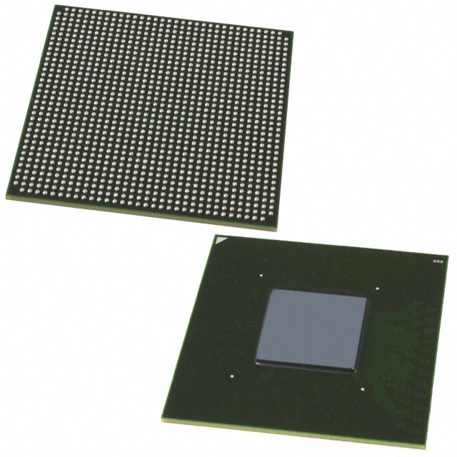
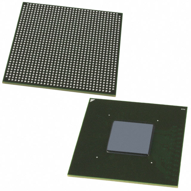
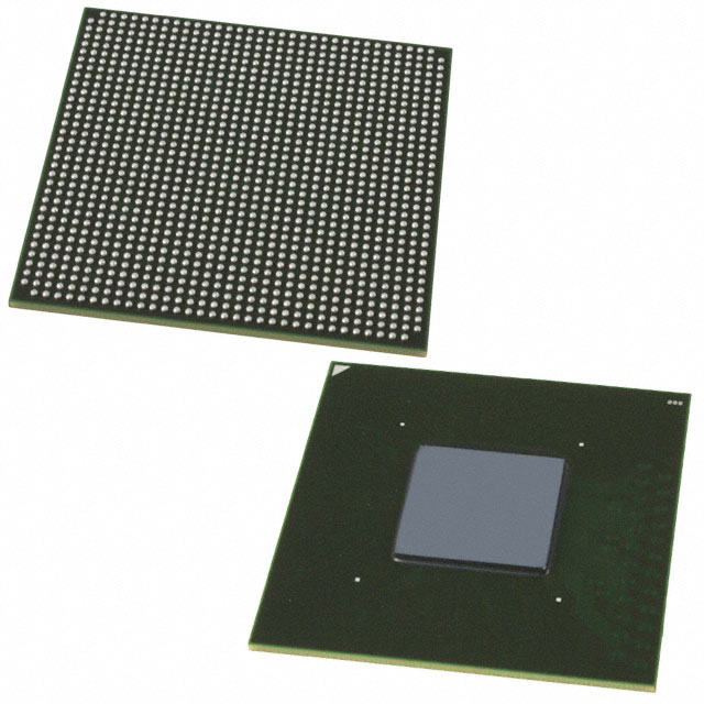
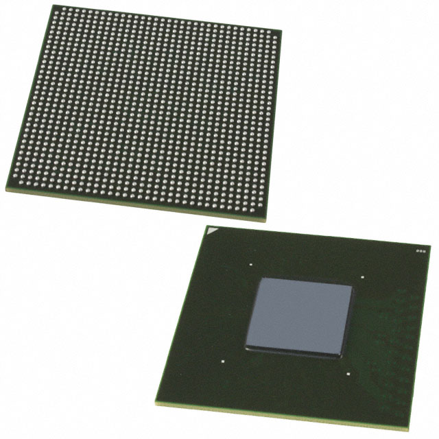
Arria V GX Field Programmable Gate Array (FPGA) IC 544 13284352 190000 1152-BBGA, FCBGA Exposed Pad |
|---|---|
| Quantity | 1,055 Available (as of October 8, 2026) |
| Product Category | Field Programmable Gate Array (FPGA) |
|---|---|
| Manufacturer | Intel |
| Manufacturing Status | Obsolete |
| Manufacturer Standard Lead Time | Contact Us |
| Datasheet |
Specifications & Environmental
| Device Package | 1152-FBGA (35x35) | Grade | Commercial | Operating Temperature | 0°C – 85°C | ||
|---|---|---|---|---|---|---|---|
| Package / Case | 1152-BBGA, FCBGA Exposed Pad | Number of I/O | 544 | Voltage | 1.07 V - 1.13 V | ||
| Mounting Method | Surface Mount | RoHS Compliance | RoHS Compliant | REACH Compliance | REACH Unknown | ||
| Moisture Sensitivity Level | 3 (168 Hours) | Number of LABs/CLBs | 8962 | Number of Logic Elements/Cells | 190000 | ||
| Number of Gates | N/A | ECCN | 3A001A2C | HTS Code | 8542.39.0001 | ||
| Qualification | N/A | Total RAM Bits | 13284352 |
Overview of 5AGXFA5H6F35C6N – Arria V GX FPGA, 1152‑BBGA (Exposed Pad), 190,000 logic elements
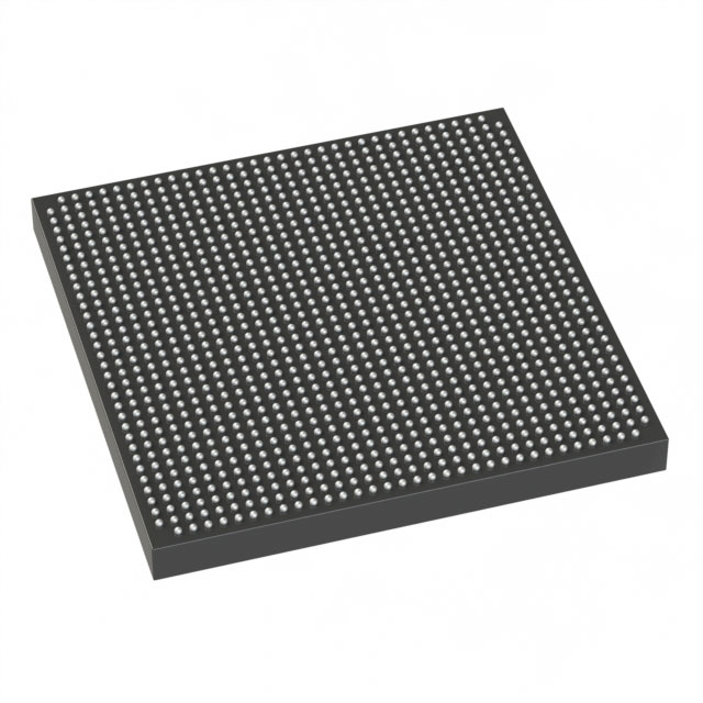
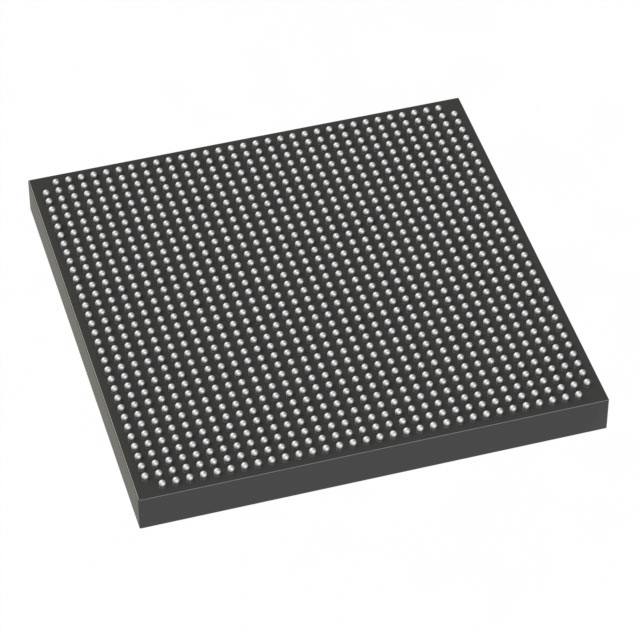
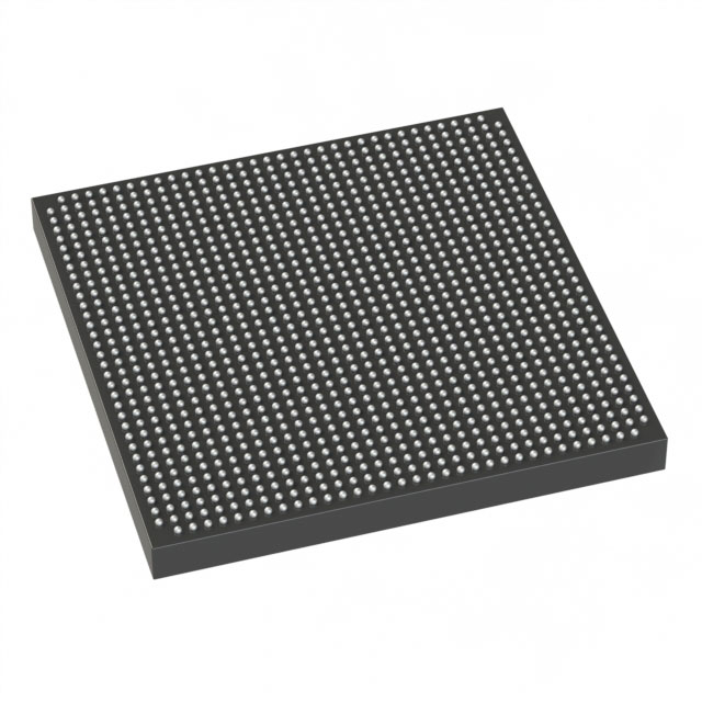
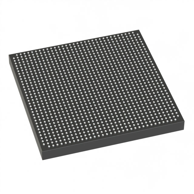
The 5AGXFA5H6F35C6N is an Intel Arria V GX field‑programmable gate array (FPGA) supplied in a 1152‑BBGA exposed‑pad surface‑mount package (supplier package: 1152‑FBGA, 35×35). It delivers high logic density with 190,000 logic elements and substantial on‑chip memory, making it suitable for commercial programmable logic applications where integration and I/O capacity matter.
Design documentation for the Arria V family covers electrical and switching characteristics, transceiver and core performance, periphery and HPS specifications, configuration, and I/O timing—supporting system‑level integration and performance verification for this device family.
Key Features
- Logic Capacity Approximately 190,000 logic elements to implement large-scale programmable logic and complex algorithms.
- Embedded Memory Approximately 13.28 Mbits of total on‑chip RAM to support buffering, lookup tables, and memory‑intensive functions.
- High I/O Count 544 user I/O pins to accommodate dense external interfaces and parallel connections.
- Package and Mounting 1152‑BBGA exposed‑pad package (supplier package 1152‑FBGA, 35×35); surface‑mount mounting for compact board integration.
- Core Voltage Core supply operating range of 1.07 V to 1.13 V for predictable power sequencing and supply design.
- Commercial Temperature Range Rated for operation from 0 °C to 85 °C (commercial grade).
- Comprehensive Documentation Arria V device datasheet provides detailed sections on electrical characteristics, switching behavior, transceiver performance, core and periphery specifications, configuration timing, and I/O timing.
- RoHS Compliant Manufactured in compliance with RoHS requirements.
Typical Applications
- High‑density programmable logic Implement large combinational and sequential logic networks requiring high logic element counts.
- Memory‑intensive designs Use the device’s approximately 13.28 Mbits of embedded RAM for buffering, packet storage, or lookup tables.
- High‑pin‑count I/O systems Support designs that require many external interfaces with the device’s 544 I/O pins.
- Compact board integration Leverage the 1152‑BBGA exposed‑pad package for space‑constrained commercial products.
Unique Advantages
- High integration density: With around 190,000 logic elements and substantial embedded RAM, the device reduces the need for external logic and memory components.
- Extensive I/O capacity: 544 I/O pins provide flexibility for complex interfacing and parallel signal routing.
- Compact BGA package: The 1152‑BBGA (1152‑FBGA, 35×35) package with exposed pad enables thermal management and board‑level compactness.
- Defined power envelope: Narrow core voltage range (1.07–1.13 V) simplifies power supply design and sequencing.
- Commercial readiness: Rated for 0 °C to 85 °C operation and RoHS compliance for commercial product requirements.
- Detailed device documentation: Datasheet coverage of electrical, timing, configuration, and performance parameters supports engineering verification and system integration.
Why Choose 5AGXFA5H6F35C6N?
The 5AGXFA5H6F35C6N Arria V GX FPGA combines high logic density, significant on‑chip memory, and a large I/O complement in a compact surface‑mount BBGA package—making it well suited for commercial applications that require dense programmable logic and extensive interfacing. Its clearly specified operating voltage range and temperature rating simplify power and thermal planning for production designs.
Backed by comprehensive Arria V device documentation covering electrical characteristics, switching and transceiver performance, configuration, and I/O timing, this device is appropriate for engineering teams focused on integration, verification, and scalable deployment in commercial systems.
Request a quote or submit an inquiry to receive pricing, availability, and ordering information for the 5AGXFA5H6F35C6N Arria V GX FPGA.





















Date Founded: 1968
Headquarters: Santa Clara, California, USA
Employees: 130,000+
Revenue: $54.23 Billion
Certifications and Memberships: ISO9001:2015, ISO14001:2015, ISO17025:2017, ISO27001:2022, ISO45001:2018, ISO50001:2018


