
5AGXMA7G4F31C4N
| Part Description |
Arria V GX Field Programmable Gate Array (FPGA) IC 384 15470592 242000 896-BBGA, FCBGA |
|---|---|
| Quantity | 517 Available (as of June 15, 2026) |
| Product Category | Field Programmable Gate Array (FPGA) |
|---|---|
| Manufacturer | Intel |
| Manufacturing Status | Obsolete |
| Manufacturer Standard Lead Time | Contact Us |
| Datasheet |
Specifications & Environmental
| Device Package | 896-FBGA (31x31) | Grade | Commercial | Operating Temperature | 0°C – 85°C | ||
|---|---|---|---|---|---|---|---|
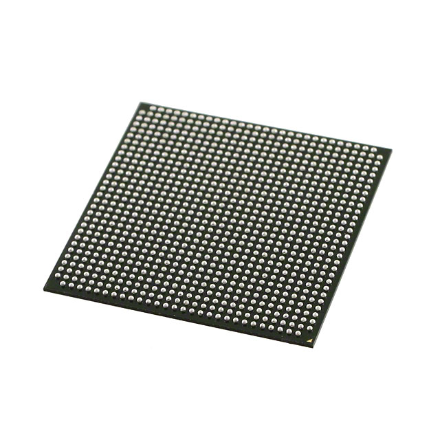
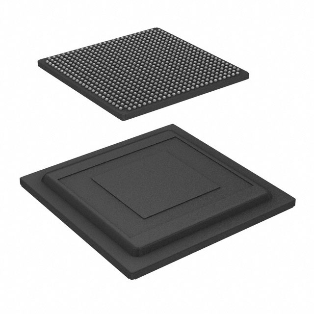
| Package / Case | 896-BBGA, FCBGA | Number of I/O | 384 | Voltage | 1.07 V - 1.13 V | ||
| Mounting Method | Surface Mount | RoHS Compliance | RoHS Compliant | REACH Compliance | REACH Unknown | ||
| Moisture Sensitivity Level | 3 (168 Hours) | Number of LABs/CLBs | 11460 | Number of Logic Elements/Cells | 242000 | ||
| Number of Gates | N/A | ECCN | 3A001A2C | HTS Code | 8542.39.0001 | ||
| Qualification | N/A | Total RAM Bits | 15470592 |
Overview of 5AGXMA7G4F31C4N – Arria V GX FPGA, 242,000 Logic Elements
The 5AGXMA7G4F31C4N is an Arria V GX Field Programmable Gate Array from Intel, packaged in a 896-ball FCBGA (896-BBGA, 31×31) surface-mount package. It delivers high logic density, substantial on-chip RAM, and a large I/O count for complex embedded and system-level designs.
Designed for commercial-grade applications, this device targets designs that require a combination of extensive programmable logic, embedded memory, and a broad I/O footprint while operating within a 1.07–1.13 V core supply range and a 0 °C to 85 °C temperature window.
Key Features
- Core Logic Approximately 242,000 logic elements provide significant programmable capacity for complex functions and custom datapaths.
- Embedded Memory Approximately 15.47 Mbits of on-chip RAM (15,470,592 bits) for large buffering, state storage, and memory-intensive logic.
- I/O Capacity 384 user I/Os to support wide parallel interfaces, multiple channels, and flexible board-level routing.
- Power and Operating Conditions Core supply range specified at 1.07 V to 1.13 V; commercial operating temperature range from 0 °C to 85 °C to match standard commercial deployments.
- Package & Mounting 896-ball FCBGA package (896-FBGA, 31×31) in an 896-BBGA case; surface-mount package intended for modern PCB assembly processes.
- Compliance RoHS compliant to meet environmental and regulatory requirements for lead-free manufacturing.
Typical Applications
- High-density programmable logic Implement complex state machines, custom accelerators, and wide datapaths using the device’s large logic-element count and on-chip RAM.
- Multi-channel I/O systems Deploy in applications that need many parallel or multiplexed signals thanks to the 384 available I/Os.
- Embedded system platforms Use for embedded control, protocol handling, and system integration where a balance of logic, memory, and I/O is required.
- Prototyping and integration Leverage the Arria V GX architecture and package density for board-level prototyping and integration into commercial products operating within standard temperature ranges.
Unique Advantages
- Large programmable capacity: The ~242k logic elements provide headroom for complex designs and future feature additions without moving to a different device family.
- Substantial on-chip memory: Approximately 15.47 Mbits of embedded RAM reduces external memory dependence for buffering and scratch storage, simplifying system design.
- High I/O count: 384 I/Os enable flexible interfacing to peripherals, sensors, and parallel buses, reducing the need for external multiplexing logic.
- Commercial-ready thermal and power envelope: Specified 1.07–1.13 V core supply and 0 °C to 85 °C rating align with typical commercial deployment requirements.
- Board-level integration: 896-ball FCBGA (31×31) surface-mount package provides a compact, high-density footprint suitable for modern PCB layouts.
- RoHS compliance: Supports lead-free manufacturing flows and environmental regulatory requirements.
Why Choose 5AGXMA7G4F31C4N?
The 5AGXMA7G4F31C4N Arria V GX FPGA balances high logic density, generous on-chip memory, and a large I/O complement in a single commercial-grade FCBGA package. It is well suited to designers and system integrators who need significant programmable resources and flexible interfacing while operating within standard commercial voltage and temperature ranges.
Backed by Intel’s Arria V family documentation and specifications, this device provides a scalable solution for mid-to-high complexity applications where integration, deterministic on-chip resources, and RoHS compliance are required.
Request a quote or submit an inquiry to get current pricing, lead time, and availability for the 5AGXMA7G4F31C4N.


Date Founded: 1968
Headquarters: Santa Clara, California, USA
Employees: 130,000+
Revenue: $54.23 Billion
Certifications and Memberships: ISO9001:2015, ISO14001:2015, ISO17025:2017, ISO27001:2022, ISO45001:2018, ISO50001:2018


