
5AGXMA7D6F27C6G
| Part Description |
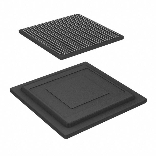
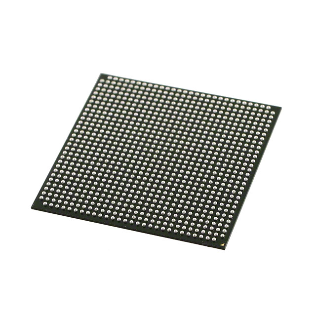
Arria V GX Field Programmable Gate Array (FPGA) IC 336 15470592 242000 672-BBGA, FCBGA |
|---|---|
| Quantity | 743 Available (as of June 15, 2026) |

| Product Category | Field Programmable Gate Array (FPGA) |
|---|---|
| Manufacturer | Intel |
| Manufacturing Status | Active |
| Manufacturer Standard Lead Time | 12 Weeks |
| Datasheet |
Specifications & Environmental
| Device Package | 672-FBGA (27x27) | Grade | Commercial | Operating Temperature | 0°C – 85°C | ||
|---|---|---|---|---|---|---|---|
| Package / Case | 672-BBGA, FCBGA | Number of I/O | 336 | Voltage | 1.07 V - 1.13 V | ||
| Mounting Method | Surface Mount | RoHS Compliance | RoHS Compliant | REACH Compliance | REACH Unaffected | ||
| Moisture Sensitivity Level | 3 (168 Hours) | Number of LABs/CLBs | 11460 | Number of Logic Elements/Cells | 242000 | ||
| Number of Gates | N/A | ECCN | PENDING ECCN | HTS Code | 0000.00.0000 | ||
| Qualification | N/A | Total RAM Bits | 15470592 |
Overview of 5AGXMA7D6F27C6G – Arria V GX FPGA, 242,000 Logic Elements, 336 I/O, 672‑FBGA
The 5AGXMA7D6F27C6G is an Intel Arria V GX family Field Programmable Gate Array (FPGA) offered in a commercial grade. This high‑density, surface‑mount FPGA provides 242,000 logic elements and approximately 15.47 Mbits of embedded RAM to support complex programmable logic, on‑chip memory, and I/O‑rich designs. Its 672‑ball FCBGA package and 336 user I/O pins make it suitable for dense board layouts requiring broad I/O connectivity.
Key Features
- Logic Capacity — 242,000 logic elements for large combinational and sequential logic implementations and complex design partitioning.
- Embedded Memory — Approximately 15.47 Mbits of on‑chip RAM to support buffering, FIFOs, and on‑chip data storage.
- I/O Resources — 336 available I/O pins to accommodate wide parallel interfaces and multiple peripheral connections.
- Package & Mounting — 672‑BBGA (FCBGA) package, supplier device package 672‑FBGA (27×27), delivered in a surface‑mount form factor for high‑density PCB assembly.
- Power Envelope — Core supply operating range specified at 1.07 V to 1.13 V for defined power and timing characteristics.
- Operating Range — Commercial temperature grade rated from 0 °C to 85 °C, suited to standard commercial environments.
- Compliance — RoHS‑compliant to meet standard environmental restrictions on hazardous substances.
Typical Applications
- High‑density programmable logic — Implement complex custom logic and state machines using 242,000 logic elements and on‑chip RAM for local storage.
- Memory‑intensive processing — Use the approximately 15.47 Mbits of embedded RAM for buffering, packet queues, and intermediate data processing.
- I/O‑centric systems — Leverage 336 I/O pins for multiple parallel interfaces, wide buses, or mixed signal front‑end connections.
Unique Advantages
- Substantial logic density: 242,000 logic elements enable large designs and extensive feature integration on a single FPGA.
- Significant on‑chip RAM: Approximately 15.47 Mbits of embedded memory reduces reliance on external memory for many buffering and staging tasks.
- Broad I/O availability: 336 I/O pins provide flexibility for high‑pin‑count interfaces without requiring additional bridge logic.
- Compact, manufacturable package: 672‑ball FCBGA in a 27×27 footprint supports high‑density PCB designs and standard surface‑mount assembly.
- Commercial grade suitability: Specified for 0 °C to 85 °C operation, aligning with typical commercial product requirements.
- Regulatory readiness: RoHS compliance helps streamline environmental compliance for product manufacturing.
Why Choose 5AGXMA7D6F27C6G?
The 5AGXMA7D6F27C6G Arria V GX FPGA combines high logic capacity, substantial embedded memory, and ample I/O in a single surface‑mount FCBGA package. Its defined core voltage range and commercial temperature rating make it a clear choice for designers who need a programmable, on‑board compute fabric with significant internal resources and flexible I/O for mid‑to‑high complexity systems.
This device is well suited to development teams and procurement groups targeting scalable FPGA integration where on‑chip RAM, logic density, and board‑level I/O count are principal selection criteria. It provides a balance of integration and manufacturability for commercial applications supported by Intel’s Arria V device family documentation.
Request a quote or submit a procurement inquiry to obtain pricing, availability, and lead‑time information for the 5AGXMA7D6F27C6G Arria V GX FPGA.


Date Founded: 1968
Headquarters: Santa Clara, California, USA
Employees: 130,000+
Revenue: $54.23 Billion
Certifications and Memberships: ISO9001:2015, ISO14001:2015, ISO17025:2017, ISO27001:2022, ISO45001:2018, ISO50001:2018


