
5AGXMA7G4F31C4G
| Part Description |
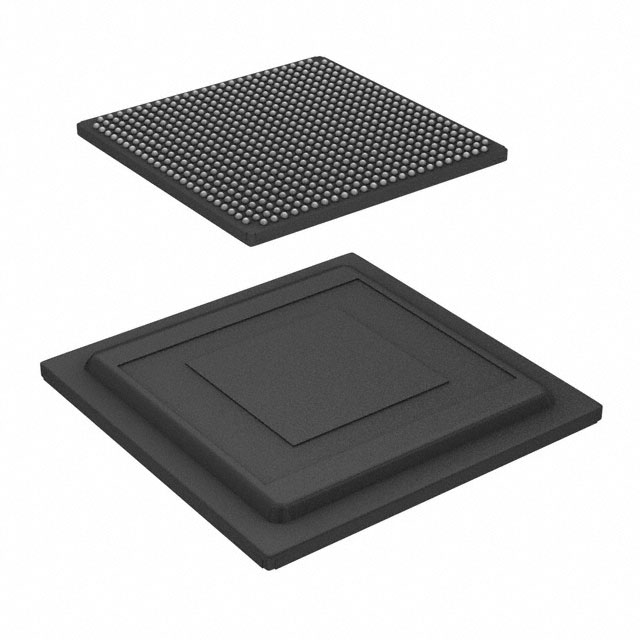
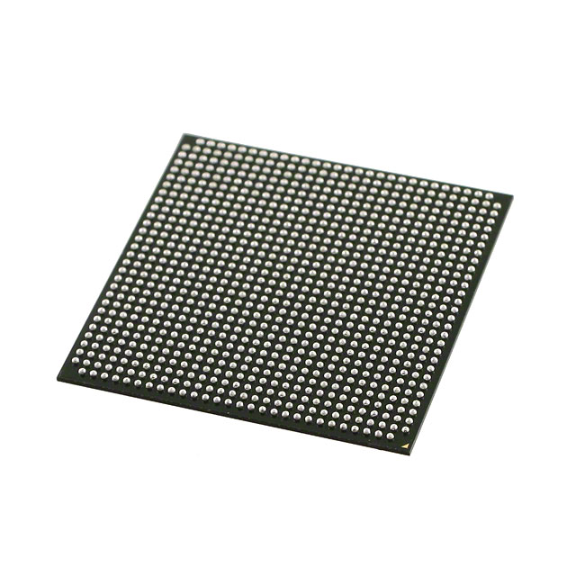
Arria V GX Field Programmable Gate Array (FPGA) IC 384 15470592 242000 896-BBGA, FCBGA |
|---|---|
| Quantity | 36 Available (as of June 18, 2026) |

| Product Category | Field Programmable Gate Array (FPGA) |
|---|---|
| Manufacturer | Intel |
| Manufacturing Status | Active |
| Manufacturer Standard Lead Time | 12 Weeks |
| Datasheet |
Specifications & Environmental
| Device Package | 896-FBGA (31x31) | Grade | Commercial | Operating Temperature | 0°C – 85°C | ||
|---|---|---|---|---|---|---|---|
| Package / Case | 896-BBGA, FCBGA | Number of I/O | 384 | Voltage | 1.07 V - 1.13 V | ||
| Mounting Method | Surface Mount | RoHS Compliance | RoHS Compliant | REACH Compliance | REACH Unaffected | ||
| Moisture Sensitivity Level | 3 (168 Hours) | Number of LABs/CLBs | 11460 | Number of Logic Elements/Cells | 242000 | ||
| Number of Gates | N/A | ECCN | PENDING ECCN | HTS Code | 0000.00.0000 | ||
| Qualification | N/A | Total RAM Bits | 15470592 |
Overview of 5AGXMA7G4F31C4G – Arria V GX Field Programmable Gate Array (FPGA) IC, 384 I/Os, 242,000 Logic Elements
The 5AGXMA7G4F31C4G is an Arria V GX Field Programmable Gate Array in an 896-BBGA (FCBGA) package designed for surface-mount assemblies. The device delivers substantial programmable logic capacity, on-chip memory, and a high I/O count for designs that require dense logic integration and flexible I/O connectivity.
With 242,000 logic elements and approximately 15.47 Mbits of embedded memory, this commercial‑grade FPGA is targeted at applications that need large programmable resources combined with a compact, high‑density package and RoHS compliance.
Key Features
- Logic Capacity Provides 242,000 logic elements to implement complex digital logic, state machines, and algorithm acceleration directly in programmable fabric.
- Embedded Memory Approximately 15.47 Mbits of on-chip RAM for buffering, lookup tables, and local data storage.
- High I/O Density 384 I/O pins support extensive interfacing to peripherals, mezzanine boards, and high‑pin-count connectors.
- Package and Mounting 896-FBGA (31×31) package in an 896-BBGA, FCBGA form factor; surface-mount mounting type for compact board-level integration.
- Power Core supply range specified at 1.07 V to 1.13 V to match system power‑rail design requirements.
- Commercial Grade Operating Range Rated for operation from 0 °C to 85 °C for typical commercial applications.
- Environmental Compliance RoHS compliant to meet common regulatory and manufacturing requirements.
Typical Applications
- Communications and Networking Implements protocol processing, packet handling, or custom interface logic where high I/O count and on-chip memory are required.
- Video and Imaging Supports image pipeline staging, buffering, and custom processing blocks using the device’s logic capacity and embedded RAM.
- Industrial Control and Automation Enables complex control algorithms and high-density I/O interfacing for factory and machine‑control systems within commercial temperature ranges.
- Prototyping and System Integration Provides a high-resource platform for validating architectures and consolidating multiple functions into a single FPGA package.
Unique Advantages
- Substantial Programmable Resources: 242,000 logic elements allow integration of complex digital subsystems on a single device, reducing board-level component count.
- Significant On‑Chip Memory: Approximately 15.47 Mbits of embedded RAM reduces reliance on external memory for buffering and real‑time data processing.
- High I/O Throughput: 384 I/Os support extensive external connectivity, enabling multi-channel interfaces and dense peripheral integration.
- Compact High‑Density Package: 896-FBGA (31×31) package provides a small footprint for designs that require a balance of density and manufacturability.
- Predictable Power Envelope: Narrow core voltage specification (1.07 V to 1.13 V) aids in power‑rail planning and thermal budgeting.
- Compliance‑Ready: RoHS compliance supports modern manufacturing and regulatory workflows.
Why Choose 5AGXMA7G4F31C4G?
This Arria V GX FPGA combines a high logic element count, substantial embedded memory, and a 384‑pin I/O complement in a surface‑mount 896‑FBGA package, making it suitable for designs that consolidate multiple functions into a single programmable device. Its commercial-grade operating range and RoHS compliance align with standard production environments.
Choose this device when you need scalable programmable capacity and dense I/O in a compact package for communications, imaging, industrial control, or system‑level prototyping where verified FPGA resources and predictable electrical requirements matter.
Request a quote or submit a procurement inquiry to receive pricing and availability for 5AGXMA7G4F31C4G and to discuss how it fits your design requirements.


Date Founded: 1968
Headquarters: Santa Clara, California, USA
Employees: 130,000+
Revenue: $54.23 Billion
Certifications and Memberships: ISO9001:2015, ISO14001:2015, ISO17025:2017, ISO27001:2022, ISO45001:2018, ISO50001:2018


