
5AGXMA7D6F27C6N
| Part Description |
Arria V GX Field Programmable Gate Array (FPGA) IC 336 15470592 242000 672-BBGA, FCBGA |
|---|---|
| Quantity | 828 Available (as of June 14, 2026) |
| Product Category | Field Programmable Gate Array (FPGA) |
|---|---|
| Manufacturer | Intel |
| Manufacturing Status | Obsolete |
| Manufacturer Standard Lead Time | Contact Us |
| Datasheet |
Specifications & Environmental
| Device Package | 672-FBGA (27x27) | Grade | Commercial | Operating Temperature | 0°C – 85°C | ||
|---|---|---|---|---|---|---|---|
| Package / Case | 672-BBGA, FCBGA | Number of I/O | 336 | Voltage | 1.07 V - 1.13 V | ||
| Mounting Method | Surface Mount | RoHS Compliance | RoHS Compliant | REACH Compliance | REACH Unknown | ||
| Moisture Sensitivity Level | 3 (168 Hours) | Number of LABs/CLBs | 11460 | Number of Logic Elements/Cells | 242000 | ||
| Number of Gates | N/A | ECCN | 3A001A2C | HTS Code | 8542.39.0001 | ||
| Qualification | N/A | Total RAM Bits | 15470592 |
Overview of 5AGXMA7D6F27C6N – Arria V GX FPGA, 672-FBGA (27×27)
The 5AGXMA7D6F27C6N is an Intel Arria V GX Field Programmable Gate Array (FPGA) supplied in a 672-ball FCBGA package. It provides a high-density programmable fabric with 242,000 logic elements and approximately 15.47 Mbits of embedded RAM, making it suitable for commercial-grade FPGA designs that require substantial on-chip logic and memory resources.
Designed for surface-mount assembly and specified for commercial temperature operation (0 °C to 85 °C), this device operates from a core supply range of 1.07 V to 1.13 V and exposes 336 I/O pins for board-level integration. Detailed electrical, switching, configuration, and I/O timing information is provided in the Arria V device datasheet.
Key Features
- Logic Capacity — 242,000 logic elements provide a large programmable fabric for complex logic implementations.
- Configurable Logic Resources — 11,460 logic blocks available for partitioning and synthesis of digital functions.
- Embedded Memory — Approximately 15.47 Mbits of on-chip RAM for buffering, FIFOs, and memory-mapped structures.
- I/O Connectivity — 336 I/O pins to support diverse peripheral interfaces and board-level signals.
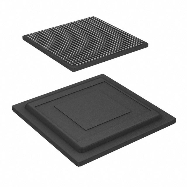
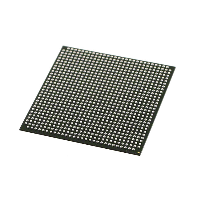
- Package — 672-ball BGA FCBGA (supplier package: 672-FBGA 27×27) optimized for high-density board layouts.
- Power and Operating Range — Core voltage supply from 1.07 V to 1.13 V; commercial operating temperature 0 °C to 85 °C.
- Mounting — Surface-mount package suitable for standard PCB assembly processes.
- Regulatory — RoHS compliant.
- Documentation — Supported by the Arria V device datasheet covering electrical characteristics, switching characteristics, configuration timing, and I/O timing.
Typical Applications
- Commercial embedded systems — Implements complex control, signal processing, or protocol logic where high logic and memory density are required.
- FPGA-based prototyping platforms — Provides a substantial logic resource pool and I/O count for hardware validation and early system integration.
- Custom digital acceleration — Allocates on-chip memory and logic elements to offload application-specific processing tasks in commercial products.
Unique Advantages
- High logic density: 242,000 logic elements enable integration of large digital designs within a single device, reducing the need for multiple FPGAs.
- Significant embedded memory: Approximately 15.47 Mbits of RAM on-chip supports buffering and complex data structures without external memory.
- Generous I/O availability: 336 I/O pins allow flexible interfacing to peripherals and daughter cards.
- Compact, board-ready package: 672-ball FCBGA (27×27) offers a compact footprint for dense PCB layouts while maintaining high pin count.
- Commercial temperature rating: Rated for 0 °C to 85 °C to match common commercial product environments.
- Comprehensive documentation: Backed by a detailed Arria V datasheet that includes electrical, switching, and configuration specifications for design validation.
Why Choose 5AGXMA7D6F27C6N?
The 5AGXMA7D6F27C6N Arria V GX FPGA combines substantial logic and embedded memory resources with a high I/O count in a compact 672-ball FCBGA package, making it well-suited for commercial designs that demand integrated programmable logic and on-chip RAM. Its defined core voltage range and commercial temperature rating provide predictable operating parameters for system designers.
Supported by Intel’s Arria V documentation, the device is appropriate for teams seeking a documented, high-capacity FPGA platform for prototyping, custom digital acceleration, and embedded system integration where on-chip resources and comprehensive datasheet guidance are important.
Request a quote or submit a purchase inquiry to obtain pricing, availability, and lead-time information for the 5AGXMA7D6F27C6N Arria V GX FPGA.


Date Founded: 1968
Headquarters: Santa Clara, California, USA
Employees: 130,000+
Revenue: $54.23 Billion
Certifications and Memberships: ISO9001:2015, ISO14001:2015, ISO17025:2017, ISO27001:2022, ISO45001:2018, ISO50001:2018


