
5AGXMB1G4F31C4N
| Part Description |
Arria V GX Field Programmable Gate Array (FPGA) IC 384 17358848 300000 896-BBGA, FCBGA |
|---|---|
| Quantity | 704 Available (as of June 15, 2026) |

| Product Category | Field Programmable Gate Array (FPGA) |
|---|---|
| Manufacturer | Intel |
| Manufacturing Status | Obsolete |
| Manufacturer Standard Lead Time | Contact Us |
| Datasheet |
Specifications & Environmental
| Device Package | 896-FBGA (31x31) | Grade | Commercial | Operating Temperature | 0°C – 85°C | ||
|---|---|---|---|---|---|---|---|
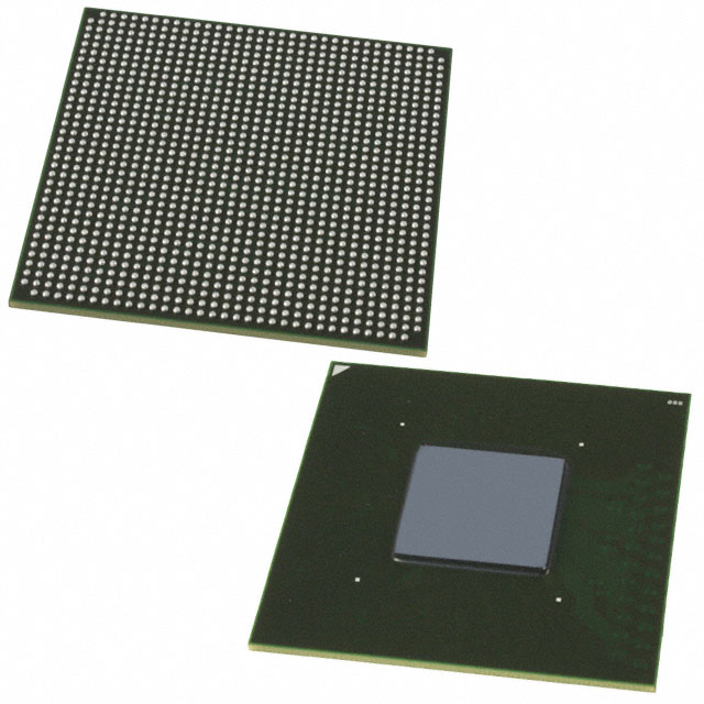
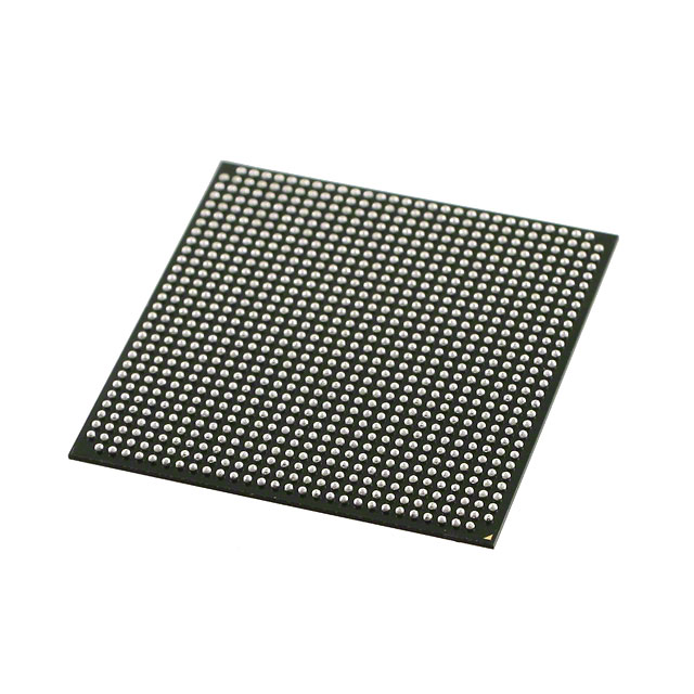
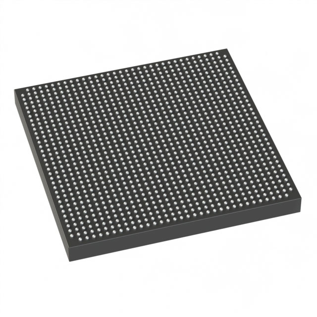
| Package / Case | 896-BBGA, FCBGA | Number of I/O | 384 | Voltage | 1.07 V - 1.13 V | ||
| Mounting Method | Surface Mount | RoHS Compliance | RoHS Compliant | REACH Compliance | REACH Unknown | ||
| Moisture Sensitivity Level | 3 (168 Hours) | Number of LABs/CLBs | 14151 | Number of Logic Elements/Cells | 300000 | ||
| Number of Gates | N/A | ECCN | 3A001A2C | HTS Code | 8542.39.0001 | ||
| Qualification | N/A | Total RAM Bits | 17358848 |
Overview of 5AGXMB1G4F31C4N – Arria V GX Field Programmable Gate Array (FPGA) IC
The 5AGXMB1G4F31C4N is an Arria V GX FPGA from Intel designed for high-density, I/O-rich digital designs. With 300,000 logic elements and a broad I/O count, this commercial-grade device supports complex system integration where on-chip logic capacity, embedded memory, and robust packaging are primary requirements.
Engineered for applications that demand large programmable logic fabrics and significant embedded memory, the device delivers a balance of capacity and integration while operating within a narrow core voltage window (1.07 V–1.13 V) and a commercial temperature range (0 °C–85 °C).
Key Features
- Logic Capacity — 300,000 logic elements to implement large-scale digital functions and complex state machines.
- Embedded Memory — Approximately 17.4 Mbits of on-chip RAM for buffering, scratch storage, and memory-intensive logic.
- I/O Resources — 384 user I/O pins to support extensive external interfaces and parallel connectivity.
- Power and Core Voltage — Core supply range of 1.07 V to 1.13 V for stable operation within specified electrical limits.
- Package and Mounting — 896-ball BGA package (896-BBGA, FCBGA) with supplier package dimensions 31 × 31 mm; surface-mount mounting type for board-level integration.
- Commercial Grade Temperature — Rated for 0 °C to 85 °C operation for standard commercial applications.
- Compliance — RoHS-compliant manufacturing to support modern regulatory and assembly requirements.
- Documented Performance — Device-level electrical and switching characteristics are covered in the Arria V device datasheet for detailed design guidance.
Typical Applications
- High-density digital processing — Implement complex logic, control engines, and custom datapaths using large logic capacity and embedded RAM.
- I/O-intensive interfaces — Support boards and modules that require many parallel or mixed-signal interfaces with 384 I/O pins.
- System integration and prototyping — Integrate multiple functions into a single programmable device for proofs-of-concept and system-level validation.
- Embedded acceleration — Offload compute-intensive logic into the FPGA fabric using the device’s significant logic and memory resources.
Unique Advantages
- Large programmable fabric: 300,000 logic elements provide the headroom to implement extensive custom logic and parallel processing blocks.
- Substantial on-chip memory: Approximately 17.4 Mbits of RAM reduces dependence on external memory for many buffering and state-storage tasks.
- High I/O density: 384 I/Os enable complex peripheral interfacing and support multiple simultaneous external connections.
- Board-level readiness: 896-ball FCBGA package and surface-mount mounting simplify PCB layout for high-density assemblies.
- Commercial operating range: Rated 0 °C–85 °C and RoHS-compliant, suitable for mainstream electronics and embedded systems.
- Tightly specified core voltage: 1.07 V–1.13 V operating window aids predictable power delivery and thermal planning.
Why Choose 5AGXMB1G4F31C4N?
The 5AGXMB1G4F31C4N Arria V GX FPGA combines a large logic fabric, significant embedded memory, and a high I/O count in a commercial-grade, RoHS-compliant BGA package. It is well suited to designs that require dense programmable logic, substantial on-chip buffering, and broad external interfacing while maintaining a clear electrical and thermal envelope defined by the datasheet.
This device fits design teams and procurement groups seeking scalable FPGA capacity with documented device characteristics for system-level integration and reliable production assembly.
Request a quote or submit an inquiry to receive pricing, availability, and lead-time information for the 5AGXMB1G4F31C4N.


Date Founded: 1968
Headquarters: Santa Clara, California, USA
Employees: 130,000+
Revenue: $54.23 Billion
Certifications and Memberships: ISO9001:2015, ISO14001:2015, ISO17025:2017, ISO27001:2022, ISO45001:2018, ISO50001:2018


