
5SEE9H40C2LN
| Part Description |
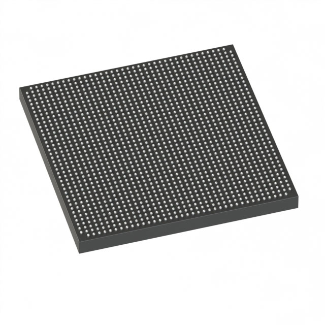
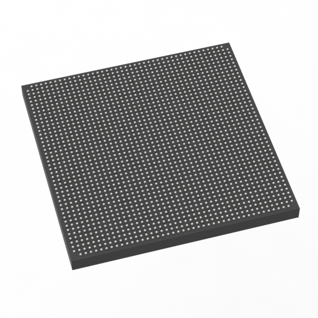
Stratix® V E Field Programmable Gate Array (FPGA) IC 696 53248000 840000 1517-BBGA, FCBGA |
|---|---|
| Quantity | 605 Available (as of June 15, 2026) |
| Product Category | Field Programmable Gate Array (FPGA) |
|---|---|
| Manufacturer | Intel |
| Manufacturing Status | Obsolete |
| Manufacturer Standard Lead Time | Contact Us |
| Datasheet |
Specifications & Environmental
| Device Package | 1517-HBGA (45x45) | Grade | Commercial | Operating Temperature | 0°C – 85°C | ||
|---|---|---|---|---|---|---|---|
| Package / Case | 1517-BBGA, FCBGA | Number of I/O | 696 | Voltage | 820 mV - 880 mV | ||
| Mounting Method | Surface Mount | RoHS Compliance | RoHS Compliant | REACH Compliance | REACH Unknown | ||
| Moisture Sensitivity Level | 3 (168 Hours) | Number of LABs/CLBs | 317000 | Number of Logic Elements/Cells | 840000 | ||
| Number of Gates | N/A | ECCN | 3A001A2C | HTS Code | 8542.39.0001 | ||
| Qualification | N/A | Total RAM Bits | 53248000 |
Overview of 5SEE9H40C2LN – Stratix® V E FPGA, 840,000 logic elements, 696 I/O, 1517-BBGA
The 5SEE9H40C2LN is a Stratix® V E Field Programmable Gate Array (FPGA) IC offering very high logic density and extensive on-chip resources in a 1517-BBGA (FCBGA) package. Built on the Stratix V architecture, this device targets compute- and memory-intensive designs where large logic capacity, abundant embedded RAM, and broad I/O are required.
Typical use cases include ASIC and system emulation, diagnostic imaging, and instrumentation, where the combination of dense logic, integrated memory blocks, DSP building blocks, and a high I/O count enables complex system functions within a single FPGA package.
Key Features
- Core and Logic Approximately 840,000 logic elements to support large, complex designs and high integration levels.
- Embedded Memory Approximately 53.25 Mbits of on-chip RAM (53,248,000 bits) provided by M20K memory blocks for high-bandwidth buffering and storage.
- DSP & Hard IP Building Blocks Includes the Stratix V family’s variable precision DSP resources and Embedded HardCopy Block support for hardened IP instantiation.
- I/O and Package 696 user I/O signals in a 1517-BBGA (FCBGA) surface-mount package (supplier package: 1517-HBGA, 45×45) for dense board-level integration.
- Power Core supply range from 0.820 V to 0.880 V, enabling designs that manage core power through specified voltage ranges.
- Operating Range & Grade Commercial grade device with an operating temperature range of 0 °C to 85 °C and RoHS compliance.
Typical Applications
- ASIC and System Emulation Use the device’s high logic capacity and memory to prototype and emulate ASIC or SoC designs at scale.
- Diagnostic Imaging Large on-chip RAM and extensive logic enable real-time image processing pipelines and high-throughput data handling.
- Instrumentation High I/O count and dense logic make the device suitable for complex test equipment and measurement systems.
- Data-Intensive Processing The combination of DSP resources and sizable embedded memory supports demanding signal- and packet-processing tasks.
Unique Advantages
- High Logic Density: Approximately 840,000 logic elements allow consolidation of large designs into a single device, reducing board-level complexity.
- Substantial On-Chip RAM: Roughly 53.25 Mbits of embedded memory supports deep buffering and high-bandwidth local storage without external DRAM.
- Extensive I/O: 696 I/O pins deliver flexible interfacing options for multi-channel systems and dense board connectivity.
- Compact, High-Density Package: 1517-BBGA (FCBGA) package supports surface-mount assembly for space-constrained, high-performance applications.
- Power Range for Core Optimization: Defined core voltage range (0.820–0.880 V) supports designs that manage core power within precise limits.
- Commercial Readiness and Compliance: Commercial temperature rating (0–85 °C) and RoHS compliance facilitate integration into mainstream electronic products.
Why Choose 5SEE9H40C2LN?
The 5SEE9H40C2LN combines the Stratix V E device architecture with high logic capacity, substantial embedded memory, and broad I/O to address complex, data- and logic-heavy applications. Its feature set is positioned for designers who need high integration in a single FPGA package for tasks such as emulation, imaging, instrumentation, and other compute-intensive systems.
As part of the Stratix V family, this device benefits from the family’s building blocks and provides a migration path within the Stratix V ecosystem, including low-risk transitions to hardened ASIC implementations where applicable.
Request a quote or submit a pricing inquiry to evaluate 5SEE9H40C2LN for your next high-density FPGA design.


Date Founded: 1968
Headquarters: Santa Clara, California, USA
Employees: 130,000+
Revenue: $54.23 Billion
Certifications and Memberships: ISO9001:2015, ISO14001:2015, ISO17025:2017, ISO27001:2022, ISO45001:2018, ISO50001:2018


