
5SEE9H40C2L
| Part Description |
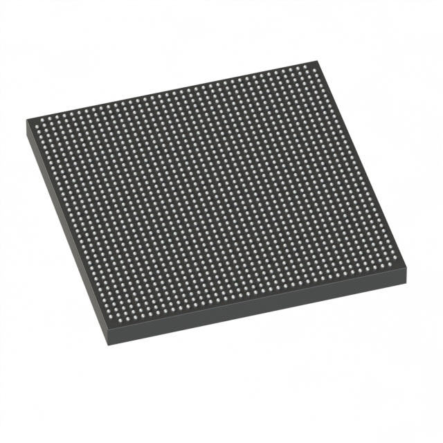
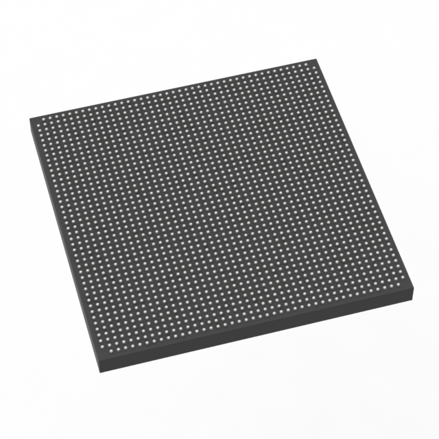
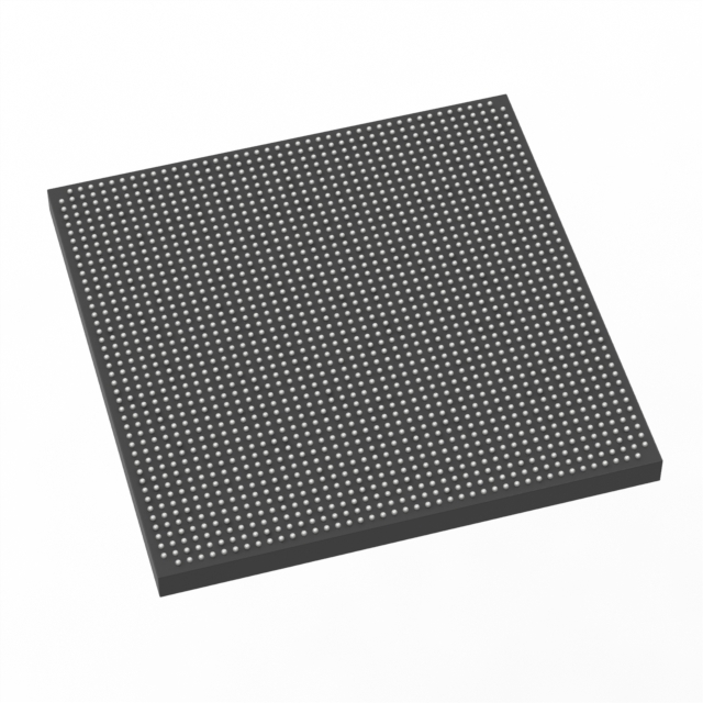
Stratix® V E Field Programmable Gate Array (FPGA) IC 696 53248000 840000 1517-BBGA, FCBGA |
|---|---|
| Quantity | 1,127 Available (as of October 7, 2026) |
| Product Category | Field Programmable Gate Array (FPGA) |
|---|---|
| Manufacturer | Intel |
| Manufacturing Status | Obsolete |
| Manufacturer Standard Lead Time | Contact Us |
| Datasheet |
Specifications & Environmental
| Device Package | 1517-HBGA (45x45) | Grade | Commercial | Operating Temperature | 0°C – 85°C | ||
|---|---|---|---|---|---|---|---|
| Package / Case | 1517-BBGA, FCBGA | Number of I/O | 696 | Voltage | 820 mV - 880 mV | ||
| Mounting Method | Surface Mount | RoHS Compliance | RoHS Compliant | REACH Compliance | REACH Unknown | ||
| Moisture Sensitivity Level | 3 (168 Hours) | Number of LABs/CLBs | 317000 | Number of Logic Elements/Cells | 840000 | ||
| Number of Gates | N/A | ECCN | 3A001A2C | HTS Code | 8542.39.0001 | ||
| Qualification | N/A | Total RAM Bits | 53248000 |
Overview of 5SEE9H40C2L – Stratix® V E Field Programmable Gate Array (FPGA), 840,000 logic elements
The 5SEE9H40C2L is an Intel Stratix V E variant FPGA offering high logic density and a rich set of on‑chip resources for data‑intensive and emulation applications. Built on the Stratix V family architecture, this device targets applications that require large logic capacity, substantial embedded memory, and extensive I/O integration.
Key value comes from its combination of approximately 840,000 logic elements, roughly 53.2 Mbits of embedded memory, and up to 696 I/O pins in a 1517‑BBGA FCBGA package, enabling compact, high‑capacity FPGA designs for system emulation, imaging, instrumentation, and other high‑density use cases.
Key Features
- Core architecture — Stratix V family features an enhanced adaptive logic module (ALM) architecture and a comprehensive fabric clocking network, delivering the architectural building blocks used in this E‑device variant.
- Logic capacity — Approximately 840,000 logic elements, optimized for designs that require high gate counts and complex logic integration.
- Embedded memory — Approximately 53.2 Mbits of on‑chip RAM, provided by M20K memory blocks for large buffer, table, and state‑storage requirements.
- DSP and timing resources — Includes variable‑precision DSP blocks and fractional PLL capabilities as part of the Stratix V feature set for precision signal processing and clock management.
- I/O and connectivity — Up to 696 I/O pins to support dense peripheral and interface requirements in board designs.
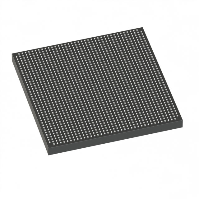
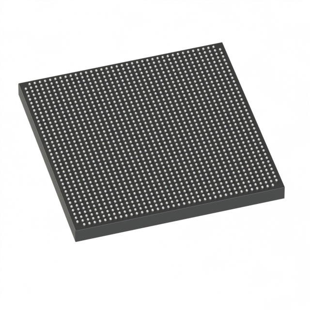
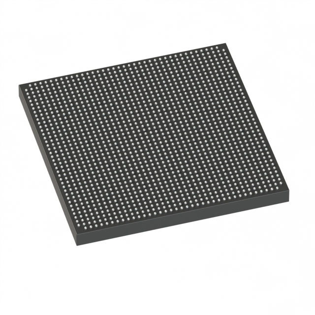
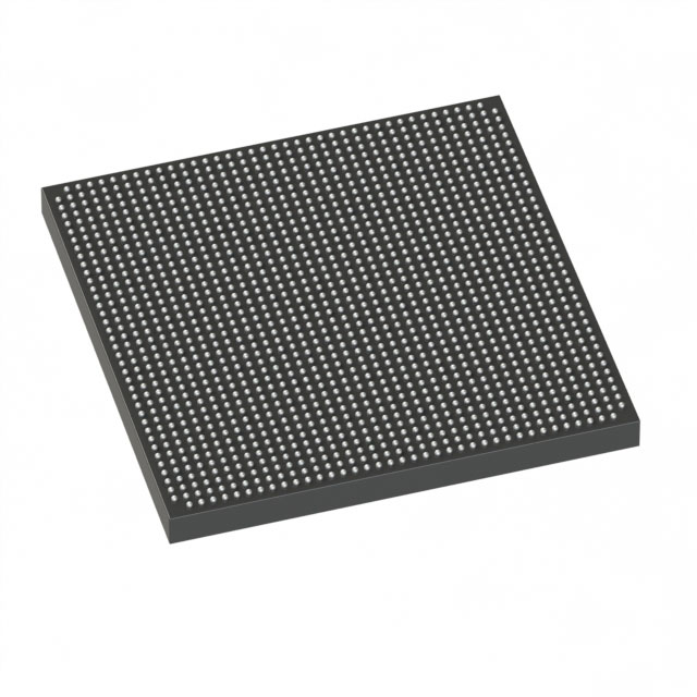
- Package and mounting — 1517‑BBGA (FCBGA) package, supplier device package listed as 1517‑HBGA (45×45); surface‑mount device suitable for compact system boards.
- Power — Core supply range specified at 820 mV to 880 mV for precise power budgeting in system designs.
- Operating range and compliance — Commercial grade operation from 0 °C to 85 °C and RoHS‑compliant.
- Family capabilities — As part of the Stratix V family, incorporates family innovations such as integrated hard IP blocks and support for high‑speed transceiver technology available within the family.
Typical Applications
- System and ASIC emulation — High logic density and large embedded memory make this device suitable for prototyping and emulation workflows where gate counts and on‑chip storage are critical.
- Diagnostic imaging — Large logic and memory resources support real‑time image processing pipelines and complex data handling in imaging instrumentation.
- Test and measurement instrumentation — Extensive I/O and programmable logic allow integration of custom data acquisition, pre‑processing, and control functions in compact instrument designs.
- Data‑intensive processing — The device’s DSP blocks and memory resources support compute‑heavy signal processing and buffering tasks in applications that demand dense logic and deterministic performance.
Unique Advantages
- High logic density: Approximately 840,000 logic elements enable consolidation of large designs into a single FPGA, reducing board count and system complexity.
- Substantial on‑chip memory: Approximately 53.2 Mbits of embedded RAM allow for large buffers and lookup structures without external memory dependence.
- Extensive I/O: Up to 696 I/O pins provide flexibility for high‑pin‑count interfaces, multiple channels, and rich peripheral integration.
- Family innovation leveraged: Benefit from Stratix V family features such as adaptive logic modules, M20K memory blocks, variable‑precision DSP blocks, and fractional PLLs for advanced timing and processing needs.
- Compact surface‑mount packaging: 1517‑BBGA (1517‑HBGA supplier package) in a 45×45 footprint supports dense board layouts while maintaining high thermal and electrical integration.
- Commercial grade, RoHS‑compliant: Designed for standard commercial operating environments and compliant with RoHS requirements for lead‑free manufacturing.
Why Choose 5SEE9H40C2L?
The 5SEE9H40C2L positions itself as a high‑density Stratix V E FPGA option for designs that require a large number of logic elements, significant embedded memory, and broad I/O resources in a single package. Its integration of Stratix V family architectural elements—such as ALMs, M20K memory blocks, DSP resources, and PLLs—helps engineers implement complex digital systems while keeping board footprint and BOM under control.
This part is suitable for engineering teams developing emulation platforms, imaging systems, instrumentation, and other data‑intensive applications that need scalable logic capacity and on‑chip memory. The device’s specified power and temperature ranges, together with RoHS compliance, support reliable deployment in commercial electronic products.
Request a quote or submit an inquiry to receive pricing, availability, and support information for the 5SEE9H40C2L FPGA.





















Date Founded: 1968
Headquarters: Santa Clara, California, USA
Employees: 130,000+
Revenue: $54.23 Billion
Certifications and Memberships: ISO9001:2015, ISO14001:2015, ISO17025:2017, ISO27001:2022, ISO45001:2018, ISO50001:2018


