
5SGSED6K2F40I3LN
| Part Description |
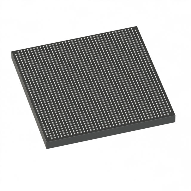
Stratix® V GS Field Programmable Gate Array (FPGA) IC 696 46080000 583000 1517-BBGA, FCBGA |
|---|---|
| Quantity | 1,985 Available (as of October 8, 2026) |
| Product Category | Field Programmable Gate Array (FPGA) |
|---|---|
| Manufacturer | Intel |
| Manufacturing Status | Obsolete |
| Manufacturer Standard Lead Time | Contact Us |
| Datasheet |
Specifications & Environmental
| Device Package | 1517-FBGA (40x40) | Grade | Industrial | Operating Temperature | -40°C – 100°C | ||
|---|---|---|---|---|---|---|---|
| Package / Case | 1517-BBGA, FCBGA | Number of I/O | 696 | Voltage | 820 mV - 880 mV | ||
| Mounting Method | Surface Mount | RoHS Compliance | RoHS Compliant | REACH Compliance | REACH Unknown | ||
| Moisture Sensitivity Level | 3 (168 Hours) | Number of LABs/CLBs | 220000 | Number of Logic Elements/Cells | 583000 | ||
| Number of Gates | N/A | ECCN | 3A001A2C | HTS Code | 8542.39.0001 | ||
| Qualification | N/A | Total RAM Bits | 46080000 |
Overview of 5SGSED6K2F40I3LN – Stratix® V GS Field Programmable Gate Array (FPGA) IC
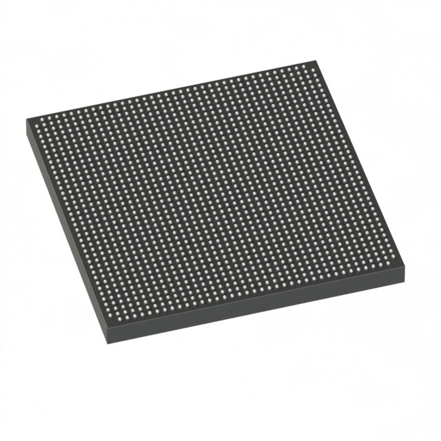
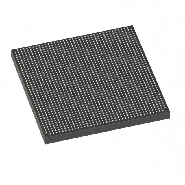
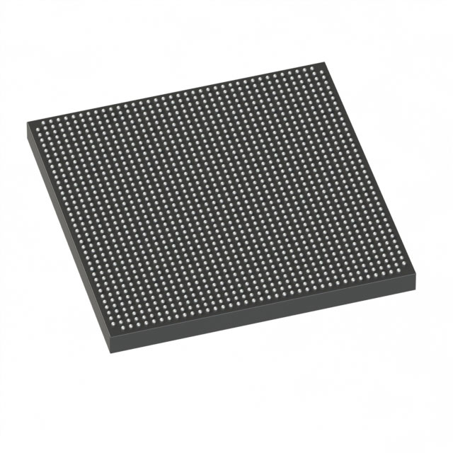
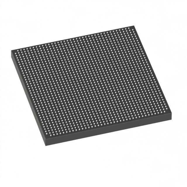
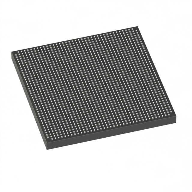
The 5SGSED6K2F40I3LN is an Intel Stratix V GS FPGA in a 1517-BBGA (40×40 FCBGA) package. It provides a large, integrated programmable fabric with extensive I/O and embedded memory, targeted at designs that require substantial on-chip logic density and flexible I/O capacity.
With 583,000 logic elements and approximately 46.08 Mbits of embedded RAM, this industrial-grade device is suitable for systems that must operate across a broad temperature range and at a defined core voltage range.
Key Features
- Logic Capacity – 583,000 logic elements and 220,000 LABs provide large-scale programmable logic resources for complex designs.
- On-chip Memory – Approximately 46.08 Mbits of embedded RAM for buffering, lookup tables, and state storage directly on-chip.
- I/O Count – 696 I/O pins to support wide parallel interfaces, multiple protocols, and extensive board-level connectivity.
- Power – Core voltage supply specified at 820 mV to 880 mV to match system power-rail planning and power budgeting requirements.
- Package – 1517-BBGA, FCBGA (supplier package: 1517-FBGA, 40×40) for high-pin-count, dense board integration.
- Temperature & Grade – Industrial grade with operating temperature range of –40 °C to 100 °C for deployment in demanding environments.
- Regulatory – RoHS compliant, supporting environmental and material-conformance requirements.
Typical Applications
- High-density logic consolidation – Use the device to implement large, consolidated digital functions where hundreds of thousands of logic elements are required.
- Protocol bridging and complex I/O – Leverage 696 I/O pins for multi-protocol interfacing, wide parallel buses, and board-level connectivity.
- On-chip buffering and data handling – Embedded RAM (≈46.08 Mbits) supports packet buffering, FIFOs, and in-line data processing.
- Industrial control systems – Industrial-grade temperature range and robust packaging make this FPGA suitable for control and automation equipment operating across wide temperatures.
Unique Advantages
- Large programmable fabric: 583,000 logic elements enable integration of complex algorithms and multiple subsystems into a single device, reducing component count.
- Significant on-chip memory: Approximately 46 Mbits of embedded RAM reduces dependence on external memory for latency-sensitive buffering.
- Extensive I/O availability: 696 I/O pins allow flexible interface routing and support for dense connector requirements.
- Industrial operating range: Rated from –40 °C to 100 °C for deployment in temperature-variable environments without additional temperature qualification statements.
- Compact high-pin-count package: 1517-BBGA (40×40 FCBGA) balances high I/O density with board-level footprint considerations.
- Material compliance: RoHS status is compliant, supporting environmental and supply-chain requirements.
Why Choose 5SGSED6K2F40I3LN?
The 5SGSED6K2F40I3LN combines a high logic element count, abundant on-chip RAM, and a large I/O complement in an industrial-grade Stratix V GS FPGA package. These measurable characteristics make it well suited for designs that consolidate multiple digital functions, implement complex data paths, or require substantial buffering and interfacing on a single device.
For engineering teams focused on scalability and robustness, this device offers a clear, specification-driven foundation: predictable core voltage range (820–880 mV), wide operating temperature window (–40 °C to 100 °C), and a high-density 1517-BBGA footprint—backed by Intel’s Stratix V device family documentation.
Request a quote or submit an inquiry to receive pricing, availability, and ordering information for the 5SGSED6K2F40I3LN. Include your required quantities and lead-time expectations to expedite our response.





















Date Founded: 1968
Headquarters: Santa Clara, California, USA
Employees: 130,000+
Revenue: $54.23 Billion
Certifications and Memberships: ISO9001:2015, ISO14001:2015, ISO17025:2017, ISO27001:2022, ISO45001:2018, ISO50001:2018


