
5SGSED8K3F40C2N
| Part Description |
Stratix® V GS Field Programmable Gate Array (FPGA) IC 696 51200000 695000 1517-BBGA, FCBGA |
|---|---|
| Quantity | 1,188 Available (as of June 14, 2026) |

| Product Category | Field Programmable Gate Array (FPGA) |
|---|---|
| Manufacturer | Intel |
| Manufacturing Status | Obsolete |
| Manufacturer Standard Lead Time | Contact Us |
| Datasheet |
Specifications & Environmental
| Device Package | 1517-FBGA (40x40) | Grade | Commercial | Operating Temperature | 0°C – 85°C | ||
|---|---|---|---|---|---|---|---|
| Package / Case | 1517-BBGA, FCBGA | Number of I/O | 696 | Voltage | 870 mV - 930 mV | ||
| Mounting Method | Surface Mount | RoHS Compliance | RoHS Compliant | REACH Compliance | REACH Unknown | ||
| Moisture Sensitivity Level | 3 (168 Hours) | Number of LABs/CLBs | 262400 | Number of Logic Elements/Cells | 695000 | ||
| Number of Gates | N/A | ECCN | 3A001A2C | HTS Code | 8542.39.0001 | ||
| Qualification | N/A | Total RAM Bits | 51200000 |
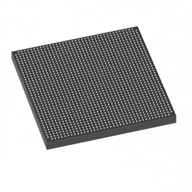
Overview of 5SGSED8K3F40C2N – Stratix® V GS Field Programmable Gate Array (FPGA), 695,000 logic elements, 1517-BBGA
The 5SGSED8K3F40C2N is a Stratix V GS series FPGA built on a 28-nm core architecture. It combines high logic density, abundant embedded memory, and a DSP- and transceiver-oriented fabric to address bandwidth- and signal-processing-centric applications.
Designed for commercial-grade systems, this device targets data-intensive and transceiver-based designs where large logic capacity, significant on-chip RAM, and extensive I/O are required.
Key Features
- Core architecture 28-nm Stratix V GS device architecture with an enhanced core and adaptive logic modules optimized for high-density logic implementations.
- Logic capacity Approximately 695,000 logic elements to implement complex PLD functions and control logic.
- Embedded memory Approximately 51.2 Mbits of on-chip RAM (51,200,000 bits) for buffering, tables, and data paths.
- DSP and transceiver focus Stratix V GS family attributes include an abundance of variable-precision DSP blocks and integrated transceivers with 14.1-Gbps capability at the family level for DSP-centric, transceiver-based designs.
- I/O density 696 user I/Os to support wide parallel interfaces and multiple serial/transceiver lanes.
- Package and mounting 1517-BBGA FCBGA package (1517-FBGA, 40×40) for high-pin-count system integration; surface-mount mounting type.
- Power and temperature Core supply range 870 mV to 930 mV and commercial operating temperature range 0 °C to 85 °C.
- Design resources Device family supports HardCopy V ASIC migration for volume production and leverages Stratix V family features such as M20K memory blocks and flexible ALM-based logic clustering (262,400 LABs reported for the device).
- Regulatory RoHS-compliant material status.
Typical Applications
- High-speed networking and switching Implement packet processing, traffic management, and 40G/100G interface logic using the device's large logic capacity and high I/O count.
- DSP-centric systems Accelerate signal processing workloads—such as broadcast processing and high-performance computing algorithms—by leveraging the Stratix V GS family’s variable-precision DSP blocks and abundant logic resources.
- Optical and backplane transceiver systems Integrate transceiver-based interfaces and backplane protocols that take advantage of family-level 14.1-Gbps transceiver capability.
- PCI Express and protocol bridging Implement protocol engines and high-bandwidth bridging, using the family’s embedded hard IP blocks and adaptable fabric for protocol offload.
Unique Advantages
- High logic and memory capacity: About 695,000 logic elements and approximately 51.2 Mbits of on-chip RAM support large, complex designs without extensive external memory.
- DSP- and transceiver-oriented architecture: Family-level variable-precision DSP blocks and integrated 14.1-Gbps transceivers tailor this device for high-performance signal-processing and high-bandwidth I/O tasks.
- Extensive I/O and package density: 696 I/Os in a 1517-BBGA package enable broad interface options and high-density system routing.
- Commercial temperature and low-voltage core: 0 °C to 85 °C operating range and 870–930 mV core supply support typical commercial deployments with low-voltage core operation.
- Production scalability: Stratix V family support for HardCopy V ASIC migration offers a defined path from FPGA prototyping to low-risk, higher-volume ASIC production.
- Standards-aligned materials: RoHS compliance supports regulated manufacturing and environmental requirements.
Why Choose 5SGSED8K3F40C2N?
5SGSED8K3F40C2N delivers a blend of high logic density, substantial embedded memory, and a transceiver- and DSP-focused architecture suitable for demanding, data- and bandwidth-oriented applications. Its 1517-BBGA package and high I/O count make it practical for systems requiring broad interfacing and dense interconnects.
This device is best suited for engineers developing high-performance networking, DSP, optical transceiver, or protocol-acceleration systems who need a commercial-grade FPGA with a clear migration path to HardCopy ASICs for production scaling.
Request a quote or submit an inquiry to receive pricing, availability, and additional ordering information for 5SGSED8K3F40C2N.


Date Founded: 1968
Headquarters: Santa Clara, California, USA
Employees: 130,000+
Revenue: $54.23 Billion
Certifications and Memberships: ISO9001:2015, ISO14001:2015, ISO17025:2017, ISO27001:2022, ISO45001:2018, ISO50001:2018


