
5SGSED8K3F40C2LN
| Part Description |
Stratix® V GS Field Programmable Gate Array (FPGA) IC 696 51200000 695000 1517-BBGA, FCBGA |
|---|---|
| Quantity | 1,026 Available (as of June 10, 2026) |

| Product Category | Field Programmable Gate Array (FPGA) |
|---|---|
| Manufacturer | Intel |
| Manufacturing Status | Obsolete |
| Manufacturer Standard Lead Time | Contact Us |
| Datasheet |
Specifications & Environmental
| Device Package | 1517-FBGA (40x40) | Grade | Commercial | Operating Temperature | 0°C – 85°C | ||
|---|---|---|---|---|---|---|---|
| Package / Case | 1517-BBGA, FCBGA | Number of I/O | 696 | Voltage | 820 mV - 880 mV | ||
| Mounting Method | Surface Mount | RoHS Compliance | RoHS Compliant | REACH Compliance | REACH Unknown | ||
| Moisture Sensitivity Level | 3 (168 Hours) | Number of LABs/CLBs | 262400 | Number of Logic Elements/Cells | 695000 | ||
| Number of Gates | N/A | ECCN | 3A001A2C | HTS Code | 8542.39.0001 | ||
| Qualification | N/A | Total RAM Bits | 51200000 |
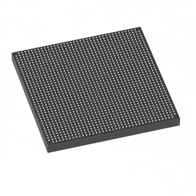
Overview of 5SGSED8K3F40C2LN – Stratix® V GS FPGA, 695,000 logic elements, 1517-BBGA
The 5SGSED8K3F40C2LN is an Intel Stratix® V GS field-programmable gate array (FPGA) designed for DSP-centric, transceiver-enabled designs. Built on a 28-nm process, this GS-variant device combines high logic density with abundant DSP resources and embedded memory to address data-intensive and high-performance signal processing applications.
Key value comes from its high logic capacity, large on-chip memory, extensive I/O, and a package suitable for surface-mount assembly, making it suitable for designs that require scalable compute, integrated transceivers, and a clear prototyping path to production ASICs.
Key Features
- Logic Capacity — 695,000 logic elements for implementing large, complex designs and high-density logic functions.
- Embedded Memory — Approximately 51.2 Mbits of on-chip RAM (51,200,000 bits) to support frame buffering, parameter storage, and intermediate data processing.
- DSP Resources — GS-family architecture provides abundant variable-precision DSP blocks; family guidance includes support for up to 3,926 18×18 or 1,963 27×27 multipliers for high-performance signal processing.
- Transceiver and I/O Capability — Up to 696 I/O pins and GS-class integrated transceivers with up to 14.1 Gbps capability per family documentation, enabling high-speed serial interfaces and backplane/optical links.
- Process and Hard IP — 28-nm TSMC technology with Embedded HardCopy Block capability for hardened IP instantiation, including PCIe Gen3/Gen2/Gen1 hardening options noted in the Stratix V family documentation.
- Power — Core supply range specified at 0.820–0.880 V to match platform power-rail design requirements.
- Package and Mounting — 1517-BBGA (FCBGA) supplier device package 1517-FBGA (40×40); surface-mount mounting for board-level integration.
- Commercial Grade — Operating temperature range 0 °C to 85 °C, RoHS-compliant.
Typical Applications
- High-performance DSP systems — Implement filtering, channelization, and complex math using the device’s variable-precision DSP blocks and large embedded memory.
- Network and optical transport — Leverage GS-family transceiver capability and high I/O count for backplane and optical interface applications in packet processing and transport equipment.
- Data-center and compute acceleration — Use the high logic capacity and on-chip RAM to accelerate data-path and network functions in compute and storage systems.
- Prototyping for ASIC migration — Prototype production designs on Stratix V GS devices and use the documented path to HardCopy V ASICs for higher-volume deployments.
Unique Advantages
- High logic density: 695,000 logic elements enable large, integration-heavy designs while reducing the need for external logic.
- Significant embedded memory: Approximately 51.2 Mbits of on-chip RAM supports buffering and state storage close to compute resources for lower latency.
- DSP-optimized architecture: GS-family variable-precision DSP blocks provide the arithmetic throughput required for demanding signal-processing pipelines.
- Extensive I/O and transceiver support: Up to 696 I/Os and GS-class transceivers enable high-bandwidth interfaces for networking and communications systems.
- Production scalability: Family-level support for Embedded HardCopy Blocks and HardCopy V ASIC path helps reduce risk when moving from prototype to volume production.
- Commercial-ready packaging: 1517-BBGA surface-mount package suitable for standard assembly processes and compact board designs.
Why Choose 5SGSED8K3F40C2LN?
The 5SGSED8K3F40C2LN positions itself as a high-density, DSP-focused Stratix V GS FPGA that balances logic capacity, on-chip memory, and high-speed I/O to support data-intensive and transceiver-based applications. Its combination of nearly 695k logic elements, large embedded RAM, and family-level DSP/transceiver capabilities makes it well suited for developers building advanced networking, broadcast, and high-performance compute systems.
For teams planning product roadmaps, the Stratix V family’s documented path to HardCopy V ASICs and the robust architecture foundations provide a clear route from prototype to production while maintaining compatibility with high-bandwidth interface requirements and commercial-temperature operation.
Request a quote or submit an inquiry to receive pricing, availability, and configuration support for the 5SGSED8K3F40C2LN.


Date Founded: 1968
Headquarters: Santa Clara, California, USA
Employees: 130,000+
Revenue: $54.23 Billion
Certifications and Memberships: ISO9001:2015, ISO14001:2015, ISO17025:2017, ISO27001:2022, ISO45001:2018, ISO50001:2018


