
5SGSED8N1F45C2G
| Part Description |
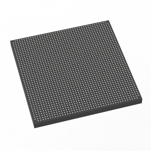
Stratix® V GS Field Programmable Gate Array (FPGA) IC 840 51200000 695000 1932-BBGA, FCBGA |
|---|---|
| Quantity | 456 Available (as of June 15, 2026) |

| Product Category | Field Programmable Gate Array (FPGA) |
|---|---|
| Manufacturer | Intel |
| Manufacturing Status | Active |
| Manufacturer Standard Lead Time | 26 Weeks |
| Datasheet |
Specifications & Environmental
| Device Package | 1932-FBGA, FC (45x45) | Grade | Commercial | Operating Temperature | 0°C – 85°C | ||
|---|---|---|---|---|---|---|---|
| Package / Case | 1932-BBGA, FCBGA | Number of I/O | 840 | Voltage | 870 mV - 930 mV | ||
| Mounting Method | Surface Mount | RoHS Compliance | RoHS Compliant | REACH Compliance | REACH Unaffected | ||
| Moisture Sensitivity Level | 3 (168 Hours) | Number of LABs/CLBs | 262400 | Number of Logic Elements/Cells | 695000 | ||
| Number of Gates | N/A | ECCN | N/A | HTS Code | N/A | ||
| Qualification | N/A | Total RAM Bits | 51200000 |
Overview of 5SGSED8N1F45C2G – Stratix® V GS Field Programmable Gate Array (FPGA) IC 840 51200000 695000 1932-BBGA, FCBGA
The 5SGSED8N1F45C2G is a Stratix V GS family Field Programmable Gate Array (FPGA) device offering very high logic capacity and I/O density in a surface-mount BGA package. It provides approximately 695,000 logic elements and approximately 51.2 Mbits of embedded memory, making it suitable for designs that require substantial on-chip programmable logic and memory resources.
Designed as a commercial-grade device, this FPGA supports a wide GPIO count and tight core supply voltage range, and is RoHS compliant. The device is supplied in a 1932-ball FCBGA package (45 × 45 mm outline) and is intended for applications requiring dense integration and high I/O connectivity within the specified commercial temperature range.
Key Features
- Large Logic Capacity — Approximately 695,000 logic elements to implement complex digital designs and high-density programmable logic.
- Embedded Memory — Approximately 51.2 Mbits of on-chip RAM for data buffering, state storage, and memory-intensive functions.
- High I/O Count — 840 user I/O pins to support wide parallel interfaces and large connector requirements.
- Package and Mounting — Surface-mount 1932-BBGA (also referenced as 1932-FBGA, FC 45×45 mm) delivering high pin-count in a compact ball-grid array.
- Power and Voltage — Core supply range specified from 870 mV to 930 mV for integration with precision power rails.
- Commercial Temperature Grade — Rated for operation from 0 °C to 85 °C for standard commercial-environment deployments.
- Regulatory — RoHS compliant.
Typical Applications
- High‑density FPGA designs — Implement large-scale logic, complex state machines, and custom accelerators using the device’s substantial logic and memory resources.
- High‑I/O systems — Support wide parallel interfaces, multi-lane connectors, or board-level I/O expansion with 840 available I/Os.
- On‑chip buffering and data handling — Use the approximately 51.2 Mbits of embedded RAM for packet buffering, frame storage, or intermediate data processing.
Unique Advantages
- High integration density: Large logic element count and significant embedded memory reduce the need for external components and simplify system partitioning.
- Extensive I/O capability: 840 I/Os enable complex board-level interfacing and flexible pin assignment for large connectivity requirements.
- Compact, high‑pin package: 1932-ball FCBGA (45×45 mm) provides very high pin count within a standard BGA footprint for dense PCB designs.
- Commercial temperature and RoHS compliance: Designed for standard commercial environments while meeting RoHS environmental requirements.
- Controlled core supply range: Defined 870 mV–930 mV core voltage specification supports precise power-supply planning and margining.
Why Choose 5SGSED8N1F45C2G?
The 5SGSED8N1F45C2G positions itself as a high-capacity Stratix V GS FPGA for commercial applications that need extensive programmable logic, on-chip memory, and very high I/O counts in a compact ball-grid package. Its combination of approximately 695,000 logic elements, approximately 51.2 Mbits of embedded RAM, and 840 I/Os makes it suitable for designs that demand large internal resources and dense connectivity.
For engineering teams targeting scalable, high-density programmable solutions, this device delivers measurable on-chip resources and well-defined electrical and mechanical specifications for straightforward system integration and supply-chain planning.
Request a quote or submit a procurement inquiry to get pricing and availability for the 5SGSED8N1F45C2G.


Date Founded: 1968
Headquarters: Santa Clara, California, USA
Employees: 130,000+
Revenue: $54.23 Billion
Certifications and Memberships: ISO9001:2015, ISO14001:2015, ISO17025:2017, ISO27001:2022, ISO45001:2018, ISO50001:2018


