
5SGSED8K3F40I4N
| Part Description |
Stratix® V GS Field Programmable Gate Array (FPGA) IC 696 51200000 695000 1517-BBGA, FCBGA |
|---|---|
| Quantity | 1,994 Available (as of October 8, 2026) |
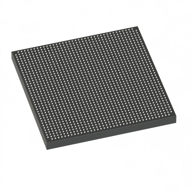
| Product Category | Field Programmable Gate Array (FPGA) |
|---|---|
| Manufacturer | Intel |
| Manufacturing Status | Obsolete |
| Manufacturer Standard Lead Time | Contact Us |
| Datasheet |
Specifications & Environmental
| Device Package | 1517-FBGA (40x40) | Grade | Industrial | Operating Temperature | -40°C – 100°C | ||
|---|---|---|---|---|---|---|---|
| Package / Case | 1517-BBGA, FCBGA | Number of I/O | 696 | Voltage | 820 mV - 880 mV | ||
| Mounting Method | Surface Mount | RoHS Compliance | RoHS Compliant | REACH Compliance | REACH Unknown | ||
| Moisture Sensitivity Level | 3 (168 Hours) | Number of LABs/CLBs | 262400 | Number of Logic Elements/Cells | 695000 | ||
| Number of Gates | N/A | ECCN | 3A001A2C | HTS Code | 8542.39.0001 | ||
| Qualification | N/A | Total RAM Bits | 51200000 |
Overview of 5SGSED8K3F40I4N – Stratix V GS FPGA, 695000 Logic Elements, 1517-FBGA
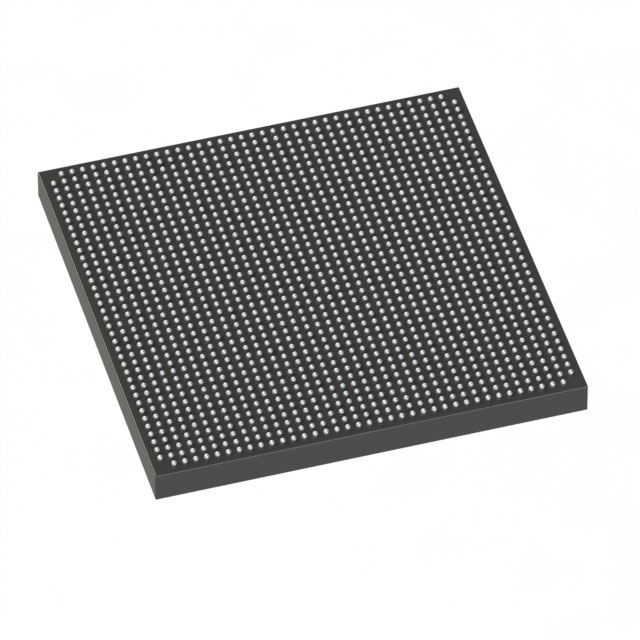
The 5SGSED8K3F40I4N is a Stratix® V GS Field Programmable Gate Array (FPGA) in a 1517-ball FCBGA package, specified for industrial operation. It delivers high logic density and on‑chip memory combined with a large I/O count for complex, high‑pin‑count designs.
Built for industrial temperature environments, this device targets applications that require extensive programmable logic, substantial embedded RAM, and a high number of I/O connections while operating from a low-voltage core supply.
Key Features
- Core Logic – 695,000 logic elements to support large-scale FPGA implementations and complex logic designs.
- Embedded Memory – Approximately 51.2 Mbits of on‑chip RAM for buffering, FIFOs, and local data storage.
- I/O Capacity – 696 I/O pins to support high-pin-count boards and multiple peripheral interfaces.
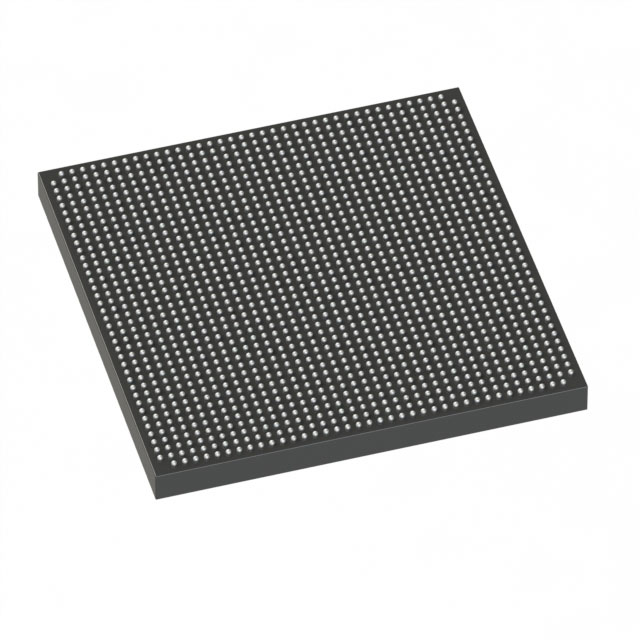
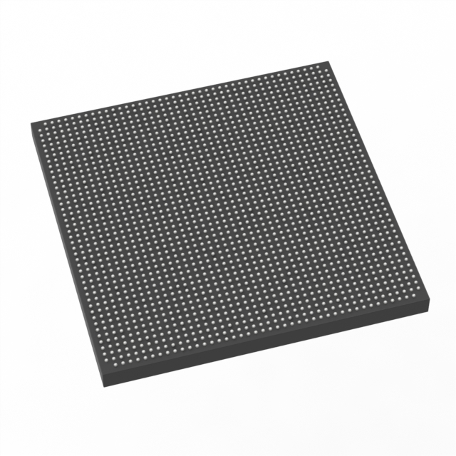
- Package – 1517‑BBGA (Supplier Device Package: 1517‑FBGA, 40 × 40) surface-mount package suitable for compact, dense board layouts.
- Power – Core voltage supply range of 820 mV to 880 mV to match low-voltage power architectures.
- Temperature Range – Industrial operating temperature from −40 °C to 100 °C for robust field deployment.
- Compliance – RoHS‑compliant manufacturing.
Typical Applications
- Industrial Control – Implement custom logic, real‑time processing, and I/O aggregation in industrial automation systems within the specified temperature range.
- High‑Density Logic Systems – Replace or consolidate multiple discrete components with programmable logic using the device’s large logic element and embedded memory resources.
- Board‑level Signal Aggregation – Use the extensive I/O count for multi‑channel interfacing, sensor aggregation, or carrier board designs that require many external connections.
Unique Advantages
- High Logic Density: 695,000 logic elements provide headroom for complex IP, algorithms, and parallel processing structures.
- Substantial On‑Chip Memory: Approximately 51.2 Mbits of embedded RAM reduce external memory dependency and improve data throughput.
- Large I/O Footprint: 696 I/O pins enable flexible interfacing with multiple peripherals and high‑pin‑count connectors.
- Industrial Temperature Rating: Specified operation from −40 °C to 100 °C supports deployment in harsh and temperature‑variable environments.
- Low‑Voltage Core: Core supply between 0.82 V and 0.88 V aligns with modern power budgets for efficient system design.
- Compact FCBGA Package: 1517‑FBGA (40 × 40) package allows dense board layouts while providing the pin count required for complex designs.
Why Choose 5SGSED8K3F40I4N?
The 5SGSED8K3F40I4N positions itself as a high‑density, industrial‑grade Stratix V GS FPGA that combines large programmable logic capacity with significant embedded memory and an extensive I/O complement. Its low-voltage core and FCBGA package make it suitable for demanding designs where board space, power efficiency, and rugged temperature operation are required.
This device is well suited for engineering teams implementing large-scale programmable logic, custom hardware acceleration, or multi‑interface aggregation who need a verified FPGA building block with documented electrical characteristics and industrial qualification.
Request a quote for the 5SGSED8K3F40I4N today to discuss availability and volume pricing for your project requirements.




















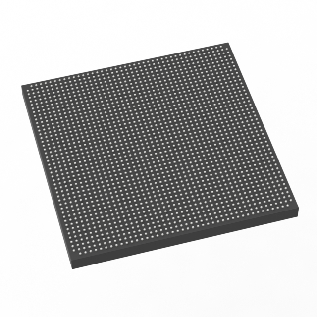
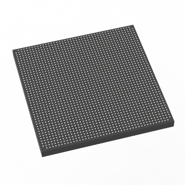
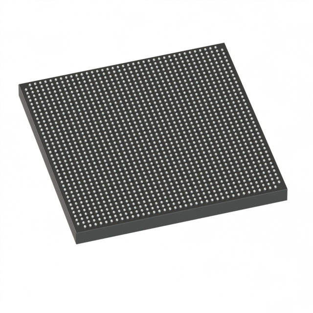

Date Founded: 1968
Headquarters: Santa Clara, California, USA
Employees: 130,000+
Revenue: $54.23 Billion
Certifications and Memberships: ISO9001:2015, ISO14001:2015, ISO17025:2017, ISO27001:2022, ISO45001:2018, ISO50001:2018


