
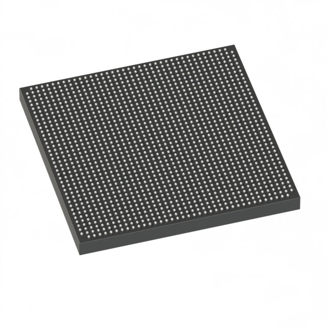
5SGSED8N1F45C2LN
| Part Description |
Stratix® V GS Field Programmable Gate Array (FPGA) IC 840 51200000 695000 1932-BBGA, FCBGA |
|---|---|
| Quantity | 862 Available (as of June 15, 2026) |

| Product Category | Field Programmable Gate Array (FPGA) |
|---|---|
| Manufacturer | Intel |
| Manufacturing Status | Obsolete |
| Manufacturer Standard Lead Time | Contact Us |
| Datasheet |
Specifications & Environmental
| Device Package | 1932-FBGA, FC (45x45) | Grade | Commercial | Operating Temperature | 0°C – 85°C | ||
|---|---|---|---|---|---|---|---|
| Package / Case | 1932-BBGA, FCBGA | Number of I/O | 840 | Voltage | 820 mV - 880 mV | ||
| Mounting Method | Surface Mount | RoHS Compliance | RoHS Compliant | REACH Compliance | REACH Unknown | ||
| Moisture Sensitivity Level | 3 (168 Hours) | Number of LABs/CLBs | 262400 | Number of Logic Elements/Cells | 695000 | ||
| Number of Gates | N/A | ECCN | 3A001A2C | HTS Code | 8542.39.0001 | ||
| Qualification | N/A | Total RAM Bits | 51200000 |
Overview of 5SGSED8N1F45C2LN – Stratix® V GS FPGA, 695,000 Logic Elements, 1932-BBGA
The 5SGSED8N1F45C2LN is an Intel Stratix V GS field-programmable gate array (FPGA) offered in a 1932‑BBGA FCBGA package. This device combines large logic capacity, abundant embedded memory, and GS-class DSP/transceiver resources to address transceiver-based, DSP-centric, and data‑intensive applications.
Designed for commercial-temperature systems, the device targets high-throughput and signal-processing use cases where a high I/O count, substantial on-chip RAM, and configurable DSP resources are required.
Key Features
- Logic Capacity Approximately 695,000 logic elements for complex programmable logic and system integration.
- Embedded Memory Approximately 51.2 Mbits of on-chip RAM, implemented with M20K embedded memory blocks for large buffering and data storage.
- Variable-Precision DSP Blocks GS-class variable-precision DSP resources supporting up to 3,926 18×18 or 1,963 27×27 multipliers for high-precision signal processing.
- Integrated Transceivers Integrated transceivers with 14.1 Gbps data-rate capability for backplane and optical-interface links (GS variant capability).
- I/O and Packaging 840 general-purpose I/O pins in a 1932‑BBGA package; supplier package listed as 1932‑FBGA, FC (45 × 45). Surface-mount mounting type.
- Power and Voltage Core supply range of 0.82 V to 0.88 V to match system power budgets.
- Temperature Grade Commercial operating range from 0 °C to 85 °C.
- Fabric and Clocking Redesigned adaptive logic modules (ALMs), multi-track routing fabric, and fractional PLLs for flexible clocking and routing (family-level architecture).
- Embedded Hard IP Embedded HardCopy block to support hardened IP instantiation such as PCIe Gen3/Gen2/Gen1.
- Compliance RoHS compliant.
Typical Applications
- High‑performance DSP systems Leverage the device’s large DSP multiplier count and extensive on-chip RAM for real-time signal processing and algorithm acceleration.
- Optical and backplane communications Use integrated 14.1 Gbps transceivers for high-speed links in optical transport and backplane interfaces.
- 40G/100G networking Deploy logic capacity and embedded memory to implement packet processing, traffic management, and protocol acceleration for data‑intensive networking systems.
- Broadcast and military communications Apply high-precision DSP and transceiver capabilities for modulation, filtering, and high‑bandwidth signaling tasks in broadcast and defense applications.
Unique Advantages
- Large programmable fabric: 695,000 logic elements enable integration of complex custom logic, state machines, and accelerators within a single device.
- Substantial on-chip memory: Approximately 51.2 Mbits of embedded RAM reduces the need for external buffering and simplifies memory architecture.
- Rich DSP resources: Up to 3,926 18×18 or 1,963 27×27 multipliers provide flexible numeric precision for demanding signal-processing algorithms.
- High I/O density: 840 I/O pins support dense peripheral interfaces and multi-lane high-speed connectivity without external expansion.
- Configurable transceiver bandwidth: Integrated transceivers (14.1 Gbps capability) offer direct support for high-speed serial links and system-level connectivity.
- Commercial temperature readiness: Rated for 0 °C to 85 °C operation for deployment in standard commercial systems.
Why Choose 5SGSED8N1F45C2LN?
The 5SGSED8N1F45C2LN combines a large logic footprint, significant on-chip RAM, dense I/O, and GS-class DSP/transceiver resources to deliver a highly capable platform for transceiver-based, DSP-centric, and data-intensive designs. Its Stratix V family architecture—featuring ALMs, M20K memory blocks, fractional PLLs, and embedded HardCopy support—provides a measured balance of integration and configurability for system designers.
This device is suited for teams building complex FPGA-based subsystems in networking, communications, broadcast, and high-performance computing domains where programmable logic, embedded memory, and high-speed serial connectivity must coexist within a commercial-temperature product.
Request a quote or submit an RFQ for the 5SGSED8N1F45C2LN to discuss availability, pricing, and lead times.


Date Founded: 1968
Headquarters: Santa Clara, California, USA
Employees: 130,000+
Revenue: $54.23 Billion
Certifications and Memberships: ISO9001:2015, ISO14001:2015, ISO17025:2017, ISO27001:2022, ISO45001:2018, ISO50001:2018


