
5SGSMD4E3H29C2LN
| Part Description |
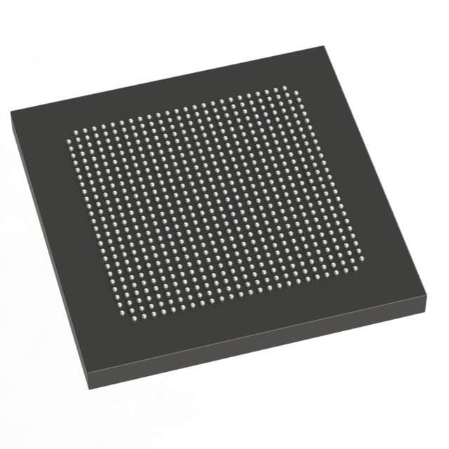
Stratix® V GS Field Programmable Gate Array (FPGA) IC 360 19456000 360000 780-BBGA, FCBGA |
|---|---|
| Quantity | 681 Available (as of June 15, 2026) |

| Product Category | Field Programmable Gate Array (FPGA) |
|---|---|
| Manufacturer | Intel |
| Manufacturing Status | Obsolete |
| Manufacturer Standard Lead Time | Contact Us |
| Datasheet |
Specifications & Environmental
| Device Package | 780-HBGA (33x33) | Grade | Commercial | Operating Temperature | 0°C – 85°C | ||
|---|---|---|---|---|---|---|---|
| Package / Case | 780-BBGA, FCBGA | Number of I/O | 360 | Voltage | 820 mV - 880 mV | ||
| Mounting Method | Surface Mount | RoHS Compliance | RoHS Compliant | REACH Compliance | REACH Unknown | ||
| Moisture Sensitivity Level | 3 (168 Hours) | Number of LABs/CLBs | 135840 | Number of Logic Elements/Cells | 360000 | ||
| Number of Gates | N/A | ECCN | 3A001A2C | HTS Code | 8542.39.0001 | ||
| Qualification | N/A | Total RAM Bits | 19456000 |
Overview of 5SGSMD4E3H29C2LN – Stratix® V GS Field Programmable Gate Array (FPGA)
The 5SGSMD4E3H29C2LN is a Stratix V GS variant FPGA in a 780‑BBGA FCBGA package, offering a high-density, transceiver-enabled fabric designed for DSP-centric and transceiver-based systems. Built on the Stratix V family architecture, this device combines a large logic capacity with substantial on-chip memory and integrated transceivers to address bandwidth- and signal-processing-focused applications.
This commercial‑grade, surface‑mount device supports a core supply range of 820 mV to 880 mV and operates from 0 °C to 85 °C, making it suitable for volume production platforms targeting wireline, broadcast, military communications, and high-performance compute applications that require programmable DSP and transceiver resources.
Key Features
- Logic Capacity — 360,000 logic elements for dense combinational and sequential logic implementations.
- Embedded Memory — Approximately 19.5 Mbits of on-chip RAM implemented with M20K embedded memory blocks to support large buffering and state storage.
- DSP Resources — Abundant variable-precision DSP blocks supporting up to 3,926 18×18 or 1,963 27×27 multipliers for high‑precision, high‑throughput signal processing.
- Integrated Transceivers — GS devices include integrated transceivers with 14.1 Gbps data‑rate capability for backplane and optical interface applications.
- I/O and Package — 360 I/O pins in a 780-BBGA (33 × 33) package; surface-mount mounting type suitable for dense board layouts.
- Process and Core — Stratix V family device architecture based on 28‑nm process technology with 0.85 V/0.9 V class core voltages; this part specifies a 820–880 mV supply range.
- Embedded HardCopy Block — Supports Embedded HardCopy Block for hardened IP instantiation, including PCIe Gen1/Gen2/Gen3 hardening options described for the family.
- Commercial Grade & RoHS — Commercial temperature grade (0 °C to 85 °C) and RoHS compliant.
Typical Applications
- Wireline and Optical Transport — Implements transceiver and DSP functions for 40G/100G class optical systems, backplane interfaces, and packet processing.
- Broadcast and High‑Performance Video — High DSP multiplier counts and large embedded RAM support demanding video processing and format conversion tasks.
- Military Communications — Programmable DSP and transceiver resources enable high‑performance signal processing and protocol interfacing in communication systems.
- High‑Performance Computing (HPC) — Dense logic and DSP resources make the device suitable for accelerator front-ends and data‑intensive compute offload functions.
Unique Advantages
- High Logic Density: 360,000 logic elements provide headroom for complex, large-scale FPGA designs without immediate need for external logic expansion.
- Substantial On‑Chip Memory: Approximately 19.5 Mbits of embedded RAM reduce dependence on external memory for buffering and state, simplifying system design.
- Targeted DSP Capability: Thousands of variable-precision multipliers enable efficient implementation of high-precision filtering, transforms, and other signal-processing kernels.
- Integrated High‑Speed I/O: 14.1 Gbps transceiver capability and 360 I/Os support high-bandwidth interfaces and flexible board-level connectivity.
- Production‑Oriented Packaging: 780‑BBGA (33 × 33) surface‑mount package supports volume manufacturing and dense PCB integration.
- Family Hardening Path: Embedded HardCopy Block availability in the Stratix V family provides a path to hardened IP implementations for PCIe and other interfaces.
Why Choose 5SGSMD4E3H29C2LN?
The 5SGSMD4E3H29C2LN combines a large logic fabric, considerable on‑chip RAM, extensive DSP multipliers, and integrated 14.1 Gbps transceivers in a production-ready 780‑BBGA package. It is positioned for engineers and system designers building transceiver- and DSP-centric platforms where programmable performance, memory bandwidth, and interface density are key requirements.
With commercial grade temperature range, a clearly defined core supply window (820–880 mV), and RoHS compliance, this Stratix V GS device fits into volume production designs that need scalability and access to the Stratix V device family features and hardening options.
Request a quote or submit an inquiry to get pricing, availability, and lead-time details for the 5SGSMD4E3H29C2LN.


Date Founded: 1968
Headquarters: Santa Clara, California, USA
Employees: 130,000+
Revenue: $54.23 Billion
Certifications and Memberships: ISO9001:2015, ISO14001:2015, ISO17025:2017, ISO27001:2022, ISO45001:2018, ISO50001:2018


