
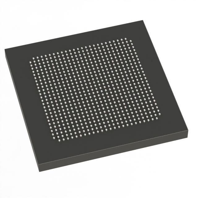
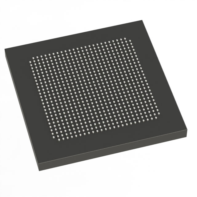
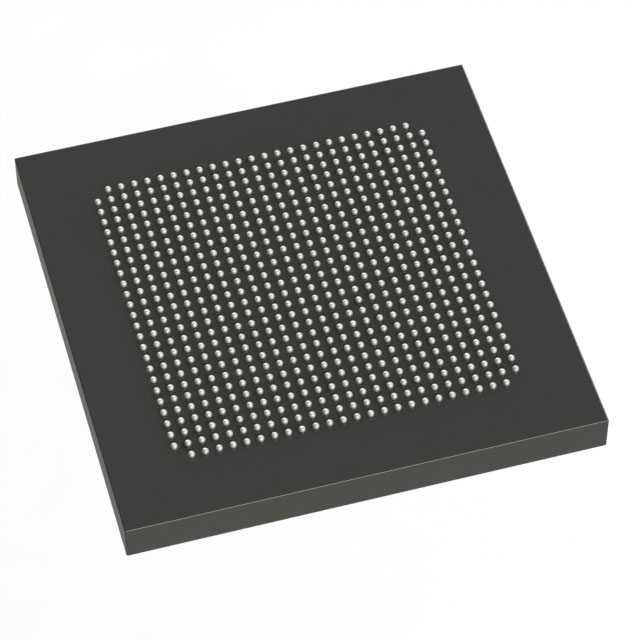
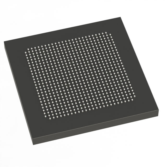
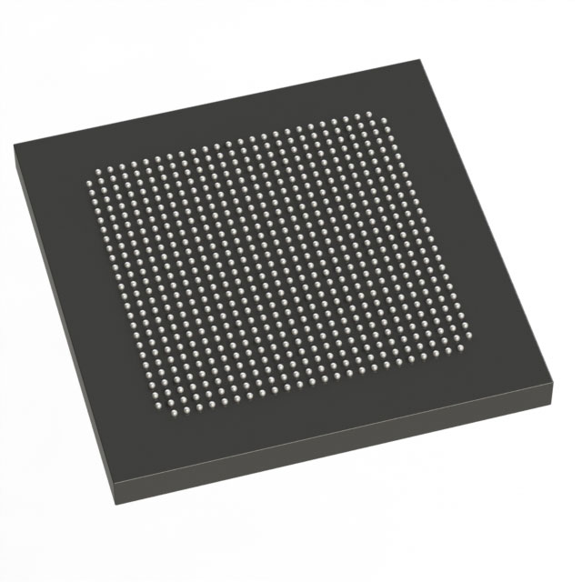
5SGSMD4E3H29C3G
| Part Description |
Stratix® V GS Field Programmable Gate Array (FPGA) IC 360 19456000 360000 780-BBGA, FCBGA |
|---|---|
| Quantity | 1,106 Available (as of October 7, 2026) |
| Product Category | Field Programmable Gate Array (FPGA) |
|---|---|
| Manufacturer | Intel |
| Manufacturing Status | Active |
| Manufacturer Standard Lead Time | 26 Weeks |
| Datasheet |
Specifications & Environmental
| Device Package | 780-HBGA (33x33) | Grade | Commercial | Operating Temperature | 0°C – 85°C | ||
|---|---|---|---|---|---|---|---|
| Package / Case | 780-BBGA, FCBGA | Number of I/O | 360 | Voltage | 820 mV - 880 mV | ||
| Mounting Method | Surface Mount | RoHS Compliance | RoHS Compliant | REACH Compliance | REACH Unaffected | ||
| Moisture Sensitivity Level | 3 (168 Hours) | Number of LABs/CLBs | 135840 | Number of Logic Elements/Cells | 360000 | ||
| Number of Gates | N/A | ECCN | N/A | HTS Code | N/A | ||
| Qualification | N/A | Total RAM Bits | 19456000 |
Overview of 5SGSMD4E3H29C3G – Stratix® V GS Field Programmable Gate Array (FPGA), 360K logic elements, 780-BBGA
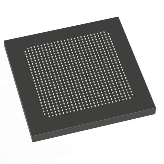
The 5SGSMD4E3H29C3G is a Stratix V GS family Field Programmable Gate Array (FPGA) in a 780-ball BGA package. It delivers high-density programmable logic, substantial on-chip RAM, and a large I/O count for advanced FPGA designs in commercial applications.
Designed as part of the Stratix V family, the device’s published documentation covers electrical and switching characteristics, including transceiver specifications and I/O timing, enabling system-level planning for power, timing, and interface requirements.
Key Features
- Core Logic Capacity 360,000 logic elements are available to implement complex custom logic, algorithmic accelerators, and large state machines.
- Embedded Memory Approximately 19.5 Mbits of on-chip RAM (19,456,000 bits) to support buffering, packet handling, and intermediate data storage.
- I/O Density 360 user I/O pins to support broad connectivity and parallel interfaces across multiple peripherals and subsystems.
- Power Core supply range from 0.820 V to 0.880 V to match platform power-rail requirements and help with system-level power budgeting.
- Package & Mounting 780-ball BGA (FCBGA) package; supplier device package listed as 780-HBGA (33×33). Surface-mount construction for standard PCB assembly processes.
- Operating Range Commercial-grade device rated for 0 °C to 85 °C operation.
- Compliance RoHS compliant for global manufacturing and environmental requirements.
- Family Documentation Stratix V device datasheet provides detailed electrical, switching, and I/O timing specifications for system design and validation.
Typical Applications
- High‑performance networking Implement packet processing, switching logic, and custom forwarding engines leveraging high logic capacity and abundant I/O.
- Telecommunications equipment Use on-chip RAM and dense logic to build protocol engines and line-rate interface controllers for telecom systems.
- Compute accelerators Deploy custom hardware accelerators and offload tasks from CPUs using the device’s sizable logic and memory resources.
- Signal processing and instrumentation Implement real-time data paths, filtering, and aggregation where large on-chip RAM and numerous I/O are required.
Unique Advantages
- Large programmable fabric: 360,000 logic elements enable implementation of substantial custom logic and parallel processing architectures on a single device.
- Significant embedded memory: Approximately 19.5 Mbits of on-chip RAM reduces external memory dependence for many buffering and temporary-storage needs.
- High I/O availability: 360 I/O pins simplify system integration with multiple high-speed interfaces or parallel buses.
- Commercial temperature support: Rated for 0 °C to 85 °C operation for mainstream commercial deployments.
- RoHS compliant: Supports environmentally conscious manufacturing and regulatory requirements.
Why Choose 5SGSMD4E3H29C3G?
This Stratix V GS FPGA balances high logic density, substantial embedded memory, and broad I/O capability in a single 780-ball BGA package, making it a practical choice for commercial designs that require on-chip resources and flexible interfacing. Its documented electrical and switching characteristics support detailed system-level design and verification.
The device is best suited for engineering teams building complex, high‑integration FPGA solutions such as networking, telecom, compute acceleration, and signal-processing systems that benefit from the combination of logic capacity, embedded RAM, and a large I/O complement.
Request a quote or submit an inquiry to discuss pricing, availability, and lead time for 5SGSMD4E3H29C3G. Our team can provide ordering information and support to evaluate the device for your design.





















Date Founded: 1968
Headquarters: Santa Clara, California, USA
Employees: 130,000+
Revenue: $54.23 Billion
Certifications and Memberships: ISO9001:2015, ISO14001:2015, ISO17025:2017, ISO27001:2022, ISO45001:2018, ISO50001:2018


