
5SGSMD4K1F40C1G
| Part Description |
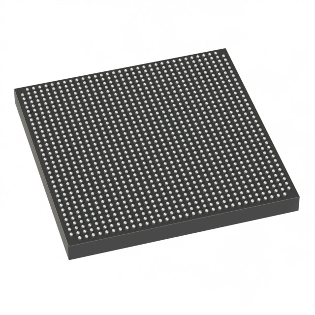
Stratix® V GS Field Programmable Gate Array (FPGA) IC 696 19456000 360000 1517-BBGA, FCBGA |
|---|---|
| Quantity | 290 Available (as of June 17, 2026) |

| Product Category | Field Programmable Gate Array (FPGA) |
|---|---|
| Manufacturer | Intel |
| Manufacturing Status | Active |
| Manufacturer Standard Lead Time | 26 Weeks |
| Datasheet |
Specifications & Environmental
| Device Package | 1517-FBGA (40x40) | Grade | Commercial | Operating Temperature | 0°C – 85°C | ||
|---|---|---|---|---|---|---|---|
| Package / Case | 1517-BBGA, FCBGA | Number of I/O | 696 | Voltage | 870 mV - 930 mV | ||
| Mounting Method | Surface Mount | RoHS Compliance | RoHS Compliant | REACH Compliance | REACH Unaffected | ||
| Moisture Sensitivity Level | 3 (168 Hours) | Number of LABs/CLBs | 135840 | Number of Logic Elements/Cells | 360000 | ||
| Number of Gates | N/A | ECCN | N/A | HTS Code | N/A | ||
| Qualification | N/A | Total RAM Bits | 19456000 |
Overview of 5SGSMD4K1F40C1G – Stratix® V GS FPGA, 360,000 logic elements
The 5SGSMD4K1F40C1G is a Stratix V GS field-programmable gate array (FPGA) IC from Intel. It delivers a high-density programmable logic fabric with a large embedded memory footprint and extensive I/O capacity, packaged in a 1517-ball FCBGA for surface-mount assembly. This device is suited to designs that require substantial logic resources, significant on-chip RAM, and high pin count within a compact package.
Key Features
- Logic Capacity Approximately 360,000 logic elements to implement large-scale digital designs and complex custom logic functions.
- Embedded Memory Approximately 19.456 Mbits of on-chip RAM for buffering, lookup tables, and state storage.
- I/O Density Up to 696 I/O pins to support wide parallel interfaces and multi-protocol connectivity.
- Package & Mounting 1517-BBGA (FCBGA) package, supplier device package 1517-FBGA (40×40); surface-mount device for PCB assembly.
- Power Supply Core voltage supply range 870 mV to 930 mV, enabling integration into low-voltage power domains.
- Operating Conditions Commercial grade with an operating temperature range of 0°C to 85°C.
- Environmental Compliance RoHS compliant.
Typical Applications
- High-density FPGA designs Deploy substantial combinational and sequential logic where large logic-element count is required.
- Memory-intensive buffering Use the device’s approximately 19.456 Mbits of embedded RAM for packet buffering, FIFOs, and large on-chip data structures.
- High-pin-count interfacing Leverage 696 I/O pins for multi-channel data aggregation, parallel buses, or dense board-level I/O routing.
Unique Advantages
- High logic integration: The device’s ~360,000 logic elements enable consolidation of complex functions onto a single FPGA, reducing external components.
- Substantial embedded memory: Approximately 19.456 Mbits of on-chip RAM supports large internal buffers and stateful processing without external memory.
- Extensive I/O capability: 696 I/O pins provide flexibility for wide data interfaces and multiple peripheral connections on a single package.
- Compact FCBGA package: The 1517-ball FCBGA (40×40) balances high integration with a manageable PCB footprint for dense system designs.
- Low-voltage core operation: Core supply range of 0.87 V–0.93 V aligns with modern low-voltage power architectures.
- Commercial-grade reliability: Rated for 0°C to 85°C operation and RoHS compliant for standard commercial applications.
Why Choose 5SGSMD4K1F40C1G?
The 5SGSMD4K1F40C1G provides a high-capacity Stratix V GS FPGA option for designs that demand a large logic fabric, significant on-chip RAM, and a high pin count in a compact FCBGA package. Its combination of approximately 360,000 logic elements, ~19.456 Mbits of embedded memory, and 696 I/Os makes it suitable for consolidating complex digital subsystems onto a single device while maintaining surface-mount packaging compatibility.
As a member of the Stratix V family, the device is supported by the published Stratix V device documentation and electrical characteristics, enabling designers to align system-level power, timing, and thermal considerations to the device’s specified limits.
Request a quote or submit an inquiry for pricing and availability to begin specifying the 5SGSMD4K1F40C1G for your next high-density FPGA design.


Date Founded: 1968
Headquarters: Santa Clara, California, USA
Employees: 130,000+
Revenue: $54.23 Billion
Certifications and Memberships: ISO9001:2015, ISO14001:2015, ISO17025:2017, ISO27001:2022, ISO45001:2018, ISO50001:2018


