
5SGSMD4K1F40C1N
| Part Description |
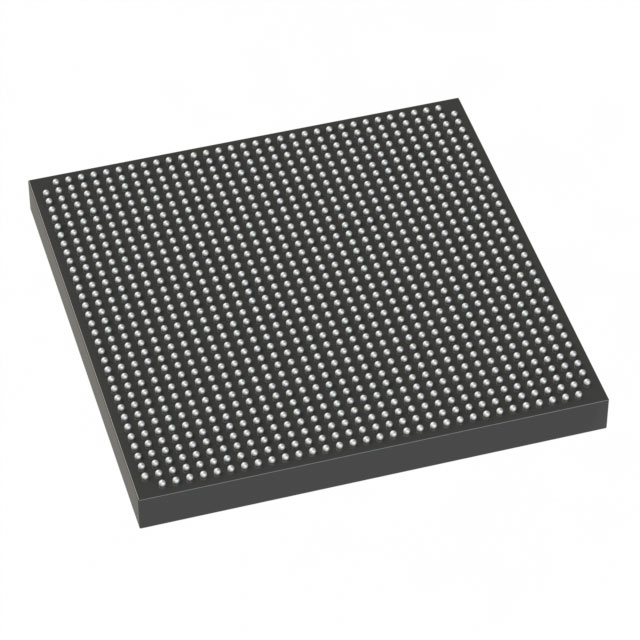
Stratix® V GS Field Programmable Gate Array (FPGA) IC 696 19456000 360000 1517-BBGA, FCBGA |
|---|---|
| Quantity | 1,401 Available (as of June 15, 2026) |

| Product Category | Field Programmable Gate Array (FPGA) |
|---|---|
| Manufacturer | Intel |
| Manufacturing Status | Obsolete |
| Manufacturer Standard Lead Time | Contact Us |
| Datasheet |
Specifications & Environmental
| Device Package | 1517-FBGA (40x40) | Grade | Commercial | Operating Temperature | 0°C – 85°C | ||
|---|---|---|---|---|---|---|---|
| Package / Case | 1517-BBGA, FCBGA | Number of I/O | 696 | Voltage | 870 mV - 930 mV | ||
| Mounting Method | Surface Mount | RoHS Compliance | RoHS Compliant | REACH Compliance | REACH Unknown | ||
| Moisture Sensitivity Level | 3 (168 Hours) | Number of LABs/CLBs | 135840 | Number of Logic Elements/Cells | 360000 | ||
| Number of Gates | N/A | ECCN | 3A001A2C | HTS Code | 8542.39.0001 | ||
| Qualification | N/A | Total RAM Bits | 19456000 |
Overview of 5SGSMD4K1F40C1N – Stratix V GS FPGA, 360,000 Logic Elements, 696 I/O
The 5SGSMD4K1F40C1N is an Intel Stratix® V GS field-programmable gate array (FPGA) in a 1517-BBGA FCBGA package. This commercial-grade device is built on the Stratix V family architecture and targets high-performance, transceiver- and DSP-centric applications.
Key on-chip resources include 360,000 logic elements, approximately 19.456 Mbits of embedded memory, and 696 I/O pins. The device operates within a core supply range of 870 mV to 930 mV and a commercial temperature range of 0 °C to 85 °C.
Key Features
- Core Architecture (Stratix V family) 28‑nm Stratix V architecture with an enhanced core and integrated hard IP blocks designed for bandwidth- and DSP-centric designs.
- Logic Capacity 360,000 logic elements for complex combinational and sequential logic implementation.
- Embedded Memory Approximately 19.456 Mbits of on-chip RAM (total RAM bits: 19,456,000) to support buffering, packet processing, and intermediate storage.
- DSP and Transceiver Capabilities As a Stratix V GS device family member, it supports abundant variable-precision DSP blocks and integrated transceivers (family-level capabilities targeted at transceiver-based DSP applications).
- I/O and Package 696 device I/O pins in a 1517-BBGA, FCBGA package (supplier device package: 1517-FBGA, 40×40) with surface-mount mounting.
- Power and Temperature Core supply range 870 mV–930 mV; commercial operating temperature range 0 °C–85 °C.
- Commercial Grade and Compliance Classified as commercial grade and RoHS compliant for standard industrial procurement and assembly processes.
Typical Applications
- High-performance DSP systems Leverage the Stratix V GS family’s variable-precision DSP resources for signal processing, filtering, and compute-heavy algorithms.
- Optical and Backplane Interfaces Family-level integrated transceivers and high I/O count support high-bandwidth serial interfaces and backplane connectivity.
- Network and Packet Processing Large logic capacity and on-chip memory enable complex packet-processing pipelines and buffering for 40G/100G applications.
- Prototyping for ASIC Migration Stratix V devices provide a low-risk prototyping path toward HardCopy ASIC implementation for higher-volume production.
Unique Advantages
- High logic density: 360,000 logic elements allow integration of large, multi-function hardware designs without immediate partitioning across multiple devices.
- Substantial embedded memory: Approximately 19.456 Mbits of on-chip RAM reduces reliance on external memory for many buffering and storage needs.
- Extensive I/O: 696 I/O pins in a compact 1517-BBGA package enable dense interfacing to high-speed PHYs, serializers, and peripheral subsystems.
- Family-level DSP and transceiver capabilities: The Stratix V GS family’s focus on variable-precision DSP and integrated transceivers aligns the device with demanding signal-processing and bandwidth-centric designs.
- Commercial temperature and RoHS compliance: Commercial operating range (0 °C–85 °C) and RoHS status simplify procurement and assembly for a broad set of applications.
- Surface-mount package: 1517-FBGA (40×40) supplier package supports standard surface-mount assembly workflows.
Why Choose 5SGSMD4K1F40C1N?
The 5SGSMD4K1F40C1N positions itself as a high-capacity Stratix V GS FPGA option for designs that demand substantial logic, on-chip memory, and extensive I/O in a commercial-grade surface-mount package. Its alignment with the Stratix V family’s DSP and transceiver feature set makes it suitable for high-throughput signal-processing, networking, and prototyping workflows that may transition to HardCopy ASICs for volume production.
Choose this device when your design requires a balance of logic capacity, embedded memory, and I/O density backed by the Stratix V architecture and Intel’s device roadmap for prototyping-to-ASIC migration.
Request a quote or submit a pricing inquiry to receive availability and ordering information for the 5SGSMD4K1F40C1N.


Date Founded: 1968
Headquarters: Santa Clara, California, USA
Employees: 130,000+
Revenue: $54.23 Billion
Certifications and Memberships: ISO9001:2015, ISO14001:2015, ISO17025:2017, ISO27001:2022, ISO45001:2018, ISO50001:2018


