
5SGSMD6K3F40C2LN
| Part Description |
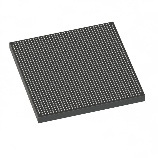
Stratix® V GS Field Programmable Gate Array (FPGA) IC 696 46080000 583000 1517-BBGA, FCBGA |
|---|---|
| Quantity | 477 Available (as of June 10, 2026) |

| Product Category | Field Programmable Gate Array (FPGA) |
|---|---|
| Manufacturer | Intel |
| Manufacturing Status | Obsolete |
| Manufacturer Standard Lead Time | Contact Us |
| Datasheet |
Specifications & Environmental
| Device Package | 1517-FBGA (40x40) | Grade | Commercial | Operating Temperature | 0°C – 85°C | ||
|---|---|---|---|---|---|---|---|
| Package / Case | 1517-BBGA, FCBGA | Number of I/O | 696 | Voltage | 820 mV - 880 mV | ||
| Mounting Method | Surface Mount | RoHS Compliance | RoHS Compliant | REACH Compliance | REACH Unknown | ||
| Moisture Sensitivity Level | 3 (168 Hours) | Number of LABs/CLBs | 220000 | Number of Logic Elements/Cells | 583000 | ||
| Number of Gates | N/A | ECCN | 3A001A2C | HTS Code | 8542.39.0001 | ||
| Qualification | N/A | Total RAM Bits | 46080000 |
Overview of 5SGSMD6K3F40C2LN – Stratix® V GS FPGA, 583,000 logic elements, ~46 Mbits RAM, 696 I/O
The 5SGSMD6K3F40C2LN is a Stratix® V GS Field Programmable Gate Array (FPGA) in a 1517-BBGA FCBGA package, intended for commercial-grade designs. This device provides a large programmable fabric with approximately 583,000 logic elements and about 46 Mbits of embedded memory, combined with a high I/O count and a compact 1517-FBGA (40×40) package.
Designed for systems that require high logic capacity, significant on-chip RAM, and extensive I/O, the device is specified for surface-mount assembly, operates at a core voltage range of 820 mV to 880 mV, and is rated for 0 °C to 85 °C operating temperature. The Stratix V device family documentation includes detailed electrical and switching characteristics, including I/O timing and programmable I/O element delays.
Key Features
- Core Logic Approximately 583,000 logic elements and 220,000 logic array blocks (LABs) provide substantial programmable logic capacity for complex designs.
- Embedded Memory Approximately 46 Mbits of on-chip RAM to support memory-intensive functions and buffering within the FPGA fabric.
- I/O Density 696 I/O pins to support multi-channel connectivity and dense system interfacing.
- Power and Voltage Specified core supply voltage range of 820 mV to 880 mV for the device core.
- Package & Mounting 1517-BBGA (FCBGA) supplier device package 1517-FBGA (40×40) in a surface-mount form factor for compact board-level integration.
- Operating Range Commercial-grade operating temperature range of 0 °C to 85 °C.
- Regulatory RoHS compliant.
- Documentation Stratix V device documentation covers electrical and switching characteristics, including I/O timing and programmable output buffer delays.
Typical Applications
- High-density digital logic Large logic element count and LAB resources support complex finite-state machines, datapaths, and custom compute blocks.
- Memory-intensive on-chip processing Approximately 46 Mbits of embedded RAM enables buffering, large FIFOs, and local data storage within the FPGA fabric.
- Multi-channel I/O systems 696 I/O pins accommodate wide parallel interfaces, sensor arrays, or multi-channel control and monitoring functions.
Unique Advantages
- Highly integrated programmable fabric: Combines large logic capacity with substantial embedded RAM to consolidate functions that would otherwise require multiple components.
- High I/O count for system integration: 696 I/O provide flexibility for dense peripheral interfacing and board-level consolidation.
- Compact FCBGA package: 1517-FBGA (40×40) package supports surface-mount assembly while maintaining a high-density silicon footprint.
- Commercial-grade reliability: Specified operating range of 0 °C to 85 °C and RoHS compliance align the device to general commercial and industrial product flows where commercial-grade parts are appropriate.
- Well-documented family: Stratix V device documentation provides detailed electrical and switching characteristics to support design validation and timing closure.
Why Choose 5SGSMD6K3F40C2LN?
The 5SGSMD6K3F40C2LN delivers a balanced combination of high programmable logic density, substantial on-chip memory, and extensive I/O in a compact FCBGA package. It is positioned for commercial designs that need to integrate substantial digital logic and memory resources onto a single FPGA to reduce board-level complexity.
With comprehensive Stratix V device documentation covering electrical and switching characteristics, designers gain access to the specifications needed for system-level integration, power planning, and I/O timing analysis—helping accelerate development and validation for complex FPGA-based systems.
Request a quote or submit an inquiry to receive pricing, availability, and support information for the 5SGSMD6K3F40C2LN.


Date Founded: 1968
Headquarters: Santa Clara, California, USA
Employees: 130,000+
Revenue: $54.23 Billion
Certifications and Memberships: ISO9001:2015, ISO14001:2015, ISO17025:2017, ISO27001:2022, ISO45001:2018, ISO50001:2018


