
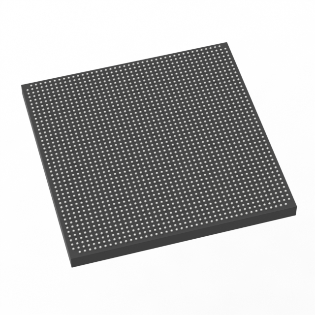
5SGSMD6N1F45C2LG
| Part Description |
Stratix® V GS Field Programmable Gate Array (FPGA) IC 840 46080000 583000 1932-BBGA, FCBGA |
|---|---|
| Quantity | 1,087 Available (as of June 10, 2026) |
| Product Category | Field Programmable Gate Array (FPGA) |
|---|---|
| Manufacturer | Intel |
| Manufacturing Status | Active |
| Manufacturer Standard Lead Time | 26 Weeks |
| Datasheet |
Specifications & Environmental
| Device Package | 1932-FBGA, FC (45x45) | Grade | Commercial | Operating Temperature | 0°C – 85°C | ||
|---|---|---|---|---|---|---|---|
| Package / Case | 1932-BBGA, FCBGA | Number of I/O | 840 | Voltage | 820 mV - 880 mV | ||
| Mounting Method | Surface Mount | RoHS Compliance | RoHS Compliant | REACH Compliance | REACH Unaffected | ||
| Moisture Sensitivity Level | 3 (168 Hours) | Number of LABs/CLBs | 220000 | Number of Logic Elements/Cells | 583000 | ||
| Number of Gates | N/A | ECCN | N/A | HTS Code | N/A | ||
| Qualification | N/A | Total RAM Bits | 46080000 |
Overview of 5SGSMD6N1F45C2LG – Stratix® V GS FPGA, 583,000 logic elements, 840 I/O
The 5SGSMD6N1F45C2LG is a Stratix® V GS field programmable gate array (FPGA) from Intel, delivered in a 1932-ball FCBGA package for surface-mount applications. It provides a high-density programmable logic fabric combined with substantial on‑chip memory and a large I/O count for advanced system designs.
Targeted at commercial-grade deployments, this device is suitable for designs that require abundant logic resources, significant embedded RAM, and extensive external interfacing within a single, compact package.
Key Features
- Logic Capacity Approximately 583,000 logic elements to implement complex, high‑density digital logic and custom datapaths.
- Embedded Memory Approximately 46 Mbits of on‑chip RAM to support buffering, FIFOs, and memory-intensive algorithms without external memory for many functions.
- High I/O Count 840 user I/O pins enable broad external connectivity for parallel interfaces, multi‑lane buses, or large sensor and actuator arrays.
- Core Voltage Core supply range is 820 mV to 880 mV, as specified for device operation.
- Package & Mounting 1932‑BBGA FCBGA (supplier device package listed as 1932‑FBGA, FC 45×45) in a surface‑mount form factor for compact board integration.
- Commercial Temperature Grade Rated for 0 °C to 85 °C operation for commercial applications.
- Programmable I/O Timing Device documentation covers I/O timing features including programmable I/O element (IOE) delay and programmable output buffer delay for timing tuning.
- Compliance RoHS‑compliant material composition.
Typical Applications
- High-density logic implementations Use the device where large amounts of programmable logic and on‑chip memory are required to implement complex state machines, custom accelerators, or layered processing pipelines.
- Data interfacing and aggregation The 840 I/O pins make this FPGA suitable for designs that consolidate multiple parallel interfaces or require extensive sensor and peripheral connectivity.
- Embedded system prototyping Leverage the device’s logic capacity and embedded RAM for validating large digital subsystems and accelerating system bring‑up in commercial projects.
Unique Advantages
- Large programmable fabric: 583,000 logic elements provide headroom for complex logic integration and multi‑function designs, reducing the need for multiple devices.
- Substantial on‑chip memory: Approximately 46 Mbits of embedded RAM minimizes dependence on external memory for many buffering and data‑processing tasks.
- Extensive I/O connectivity: 840 I/Os support dense external interfacing and simplify board‑level routing for high‑pin‑count systems.
- Compact FCBGA package: 1932‑ball FCBGA in a surface‑mount footprint enables high integration density on compact PCBs.
- Commercial temperature rating: Specified 0 °C to 85 °C operation aligns the device with a wide range of commercial applications.
- Standards‑oriented documentation: Electrical and switching characteristics, I/O timing, and power information are documented in the Stratix V device datasheet to support design verification.
Why Choose 5SGSMD6N1F45C2LG?
The 5SGSMD6N1F45C2LG delivers a combination of high logic density, large embedded memory, and a very high I/O count in a compact FCBGA package, making it well suited for commercial designs that consolidate complex digital functions and extensive external interfaces. Its documented electrical and I/O timing characteristics provide the specification detail engineers need for integration and system validation.
This Stratix V GS device is positioned for customers who require scalable programmable resources and on‑chip memory capacity while maintaining a commercial temperature profile and surface‑mount packaging for compact board designs.
Request a quote or submit an inquiry to learn more about availability and ordering for the 5SGSMD6N1F45C2LG.


Date Founded: 1968
Headquarters: Santa Clara, California, USA
Employees: 130,000+
Revenue: $54.23 Billion
Certifications and Memberships: ISO9001:2015, ISO14001:2015, ISO17025:2017, ISO27001:2022, ISO45001:2018, ISO50001:2018


