
5SGXEA4K3F35I4N
| Part Description |
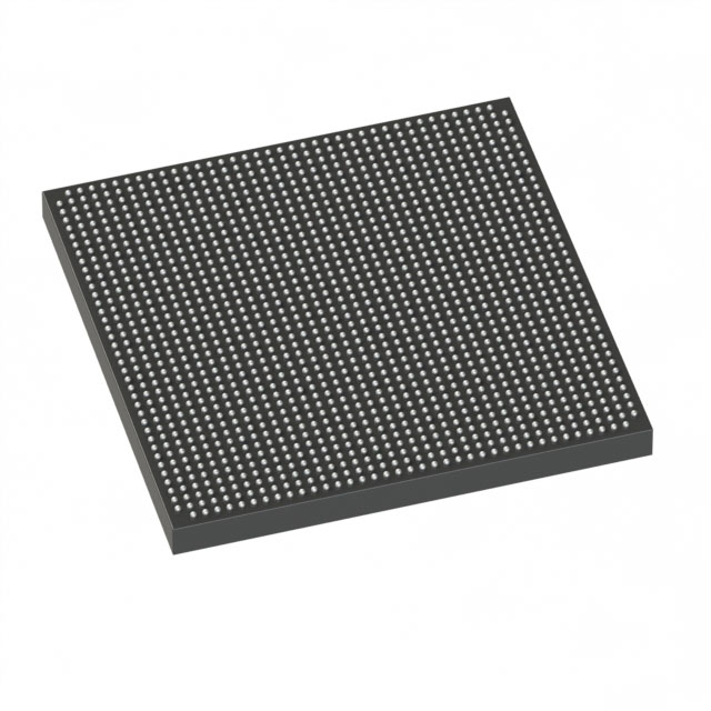
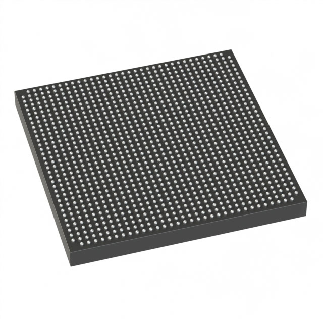
Stratix® V GX Field Programmable Gate Array (FPGA) IC 432 37888000 420000 1152-BBGA, FCBGA |
|---|---|
| Quantity | 62 Available (as of June 14, 2026) |

| Product Category | Field Programmable Gate Array (FPGA) |
|---|---|
| Manufacturer | Intel |
| Manufacturing Status | Obsolete |
| Manufacturer Standard Lead Time | Contact Us |
| Datasheet |
Specifications & Environmental
| Device Package | 1152-FBGA (35x35) | Grade | Industrial | Operating Temperature | -40°C – 100°C | ||
|---|---|---|---|---|---|---|---|
| Package / Case | 1152-BBGA, FCBGA | Number of I/O | 432 | Voltage | 820 mV - 880 mV | ||
| Mounting Method | Surface Mount | RoHS Compliance | RoHS Compliant | REACH Compliance | REACH Unknown | ||
| Moisture Sensitivity Level | 3 (168 Hours) | Number of LABs/CLBs | 158500 | Number of Logic Elements/Cells | 420000 | ||
| Number of Gates | N/A | ECCN | 3A001A2C | HTS Code | 8542.39.0001 | ||
| Qualification | N/A | Total RAM Bits | 37888000 |
Overview of 5SGXEA4K3F35I4N – Stratix® V GX FPGA (420,000 logic elements, ~37.9 Mbits RAM, 432 I/Os, 1152‑BBGA FCBGA)
The 5SGXEA4K3F35I4N is a Stratix® V GX Field Programmable Gate Array (FPGA) IC designed for high-density, programmable logic implementations. Built on the Stratix V GX family architecture, this device delivers a large logic fabric, substantial on‑chip memory, and a high I/O count for complex system integration.
Suitable for designs that require significant logic capacity, embedded memory, and broad I/O connectivity, this industrial‑grade device supports operation across an extended temperature range and a low core voltage supply for modern system power domains.
Key Features
- Core / Logic 420,000 logic elements provide a high-density programmable fabric for complex functions and custom hardware acceleration.
- Embedded Memory Approximately 37.9 Mbits of on‑chip RAM to support large buffers, state machines, and memory‑intensive logic blocks.
- I/O Capacity 432 dedicated I/O pins to interface with multiple peripherals, buses, and external devices without extensive external multiplexing.
- Power Supply Core supply range of 820 mV to 880 mV allowing integration with low‑voltage power architectures.
- Package & Mounting Supplied in a 1152‑BBGA FCBGA package (supplier device package: 1152‑FBGA 35×35) with surface‑mount capability for compact PCB layouts.
- Temperature & Grade Industrial grade operation from −40 °C to 100 °C for deployment in temperature‑challenging environments.
- Standards & Compliance RoHS compliant status for adherence to common environmental restrictions.
Typical Applications
- High‑density logic implementations Deploy large custom logic designs that require 420,000 logic elements to implement complex state machines, datapaths, or hardware accelerators.
- Memory‑intensive designs Use the approximately 37.9 Mbits of embedded memory for buffering, packet processing, or multi‑stage pipelines.
- High‑I/O systems Integrate multiple external interfaces and parallel buses using the device’s 432 I/Os to minimize external glue logic.
- Industrial and extended‑temperature applications Operate reliably in systems requiring −40 °C to 100 °C temperature support and industrial grade robustness.
Unique Advantages
- High logic density: 420,000 logic elements enable consolidation of complex functions into a single programmable device, reducing system BOM and board area.
- Large on‑chip memory: Approximately 37.9 Mbits of embedded RAM reduces reliance on external memory for many buffering and state storage needs.
- Extensive I/O: 432 I/Os simplify integration with multiple peripherals and interfaces, enabling flexible system partitioning.
- Low‑voltage core operation: 820–880 mV supply compatibility aligns with modern power architectures and helps manage power distribution.
- Robust industrial rating: Certified for operation from −40 °C to 100 °C, supporting deployment in temperature‑demanding environments.
- Compact FCBGA package: The 1152‑BBGA (1152‑FBGA, 35×35) package offers a high pin count in a package suitable for dense PCB layouts.
Why Choose 5SGXEA4K3F35I4N?
The 5SGXEA4K3F35I4N positions itself as a high‑capacity FPGA option within the Stratix V GX family, delivering a combination of large logic resources, substantial embedded memory, and high I/O count for advanced system designs. Its industrial temperature rating and low core voltage range support integration into demanding environments and modern power domains.
This device is well suited for engineers and teams building systems that require consolidation of complex functions, significant on‑chip buffering, and extensive peripheral connectivity while maintaining a compact board footprint via the 1152‑BBGA FCBGA package.
Request a quote or submit an inquiry to receive pricing and availability for the 5SGXEA4K3F35I4N. Our team can provide lead‑time information and support for procurement and integration planning.


Date Founded: 1968
Headquarters: Santa Clara, California, USA
Employees: 130,000+
Revenue: $54.23 Billion
Certifications and Memberships: ISO9001:2015, ISO14001:2015, ISO17025:2017, ISO27001:2022, ISO45001:2018, ISO50001:2018


