
5SGXEA4K3F40C3N
| Part Description |
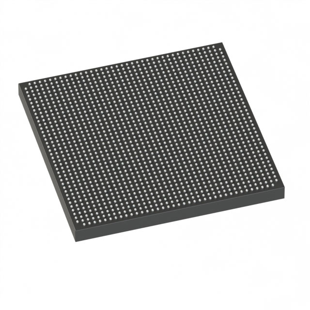
Stratix® V GX Field Programmable Gate Array (FPGA) IC 696 37888000 420000 1517-BBGA, FCBGA |
|---|---|
| Quantity | 22 Available (as of June 15, 2026) |

| Product Category | Field Programmable Gate Array (FPGA) |
|---|---|
| Manufacturer | Intel |
| Manufacturing Status | Obsolete |
| Manufacturer Standard Lead Time | Contact Us |
| Datasheet |
Specifications & Environmental
| Device Package | 1517-FBGA (40x40) | Grade | Commercial | Operating Temperature | 0°C – 85°C | ||
|---|---|---|---|---|---|---|---|
| Package / Case | 1517-BBGA, FCBGA | Number of I/O | 696 | Voltage | 820 mV - 880 mV | ||
| Mounting Method | Surface Mount | RoHS Compliance | RoHS Compliant | REACH Compliance | REACH Unknown | ||
| Moisture Sensitivity Level | 3 (168 Hours) | Number of LABs/CLBs | 158500 | Number of Logic Elements/Cells | 420000 | ||
| Number of Gates | N/A | ECCN | 3A001A2C | HTS Code | 8542.39.0001 | ||
| Qualification | N/A | Total RAM Bits | 37888000 |
Overview of 5SGXEA4K3F40C3N – Stratix® V GX Field Programmable Gate Array (FPGA) IC, 1517-BBGA FCBGA
The 5SGXEA4K3F40C3N is an Intel Stratix® V GX FPGA delivered in a 1517-BBGA FCBGA package for surface-mount applications. This device provides a high logic capacity and large on-chip memory with a broad I/O count to support complex digital designs.
With 420,000 logic elements, approximately 37.9 Mbits of embedded memory and 696 user I/Os, this commercial-grade FPGA targets designs that require large programmable logic resources, significant embedded RAM, and extensive I/O integration while operating within a 0 °C to 85 °C temperature range.
Key Features
- Core Logic 420,000 logic elements (cells) for implementing large, complex logic designs and FPGA-based systems.
- Embedded Memory Approximately 37.9 Mbits of on-chip RAM to support data buffering, FIFOs, and local storage for high-density logic functions.
- I/O Density 696 user I/O pins to accommodate wide buses, multiple interfaces, and extensive external connectivity.
- Package & Mounting 1517-BBGA, FCBGA (supplier package: 1517-FBGA, 40×40) in a surface-mount footprint for compact board integration.
- Power Core supply voltage specified at 820 mV to 880 mV to match system power-rail requirements for the FPGA core.
- Temperature & Grade Commercial grade operation with an ambient range of 0 °C to 85 °C.
- Standards Compliance RoHS compliant for regulatory and manufacturing consistency.
Typical Applications
- High-density digital systems Designs that require hundreds of thousands of logic elements and substantial embedded memory benefit from the device's logic and RAM capacity.
- Multi-interface platforms Systems that need extensive external connectivity can take advantage of the 696 available I/Os for parallel buses and multiple serial or parallel interfaces.
- Embedded processing and acceleration Local embedded memory and large logic resources support hardware acceleration blocks, custom datapaths, and on-chip buffering for performance-oriented designs.
Unique Advantages
- Large programmable fabric: 420,000 logic elements provide the headroom to implement complex algorithms and large FPGA designs without immediate part migration.
- Significant on-chip memory: Approximately 37.9 Mbits of embedded RAM reduces reliance on external memory for many buffering and caching tasks.
- Extensive I/O count: 696 I/Os enable flexible interfacing with a broad range of peripherals, sensors, and external logic devices.
- Compact BGA footprint: 1517-BBGA (1517-FBGA, 40×40) package supports high-density PCB layouts while keeping the device surface-mount compatible.
- Commercial temperature grade: Rated for 0 °C to 85 °C operation to meet standard commercial environment requirements.
- Regulatory readiness: RoHS compliance supports contemporary manufacturing and environmental requirements.
Why Choose 5SGXEA4K3F40C3N?
The 5SGXEA4K3F40C3N Stratix V GX FPGA combines substantial logic capacity, multi-megabit embedded RAM, and very high I/O density in a compact FCBGA package, making it well suited for engineers needing on-chip integration of large digital systems. Its commercial temperature rating and RoHS compliance align with standard production environments and regulatory expectations.
Designed by Intel, this device is appropriate for teams developing feature-rich FPGA implementations that require scalability of logic and memory resources while retaining flexible I/O options and a compact board footprint.
Request a quote or submit a pricing inquiry to receive availability and lead-time information for the 5SGXEA4K3F40C3N Stratix V GX FPGA.


Date Founded: 1968
Headquarters: Santa Clara, California, USA
Employees: 130,000+
Revenue: $54.23 Billion
Certifications and Memberships: ISO9001:2015, ISO14001:2015, ISO17025:2017, ISO27001:2022, ISO45001:2018, ISO50001:2018


