
5SGXEA4K3F40C3G
| Part Description |
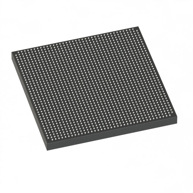
Stratix® V GX Field Programmable Gate Array (FPGA) IC 696 37888000 420000 1517-BBGA, FCBGA |
|---|---|
| Quantity | 594 Available (as of June 10, 2026) |

| Product Category | Field Programmable Gate Array (FPGA) |
|---|---|
| Manufacturer | Intel |
| Manufacturing Status | Active |
| Manufacturer Standard Lead Time | 26 Weeks |
| Datasheet |
Specifications & Environmental
| Device Package | 1517-FBGA (40x40) | Grade | Commercial | Operating Temperature | 0°C – 85°C | ||
|---|---|---|---|---|---|---|---|
| Package / Case | 1517-BBGA, FCBGA | Number of I/O | 696 | Voltage | 820 mV - 880 mV | ||
| Mounting Method | Surface Mount | RoHS Compliance | RoHS Compliant | REACH Compliance | REACH Unaffected | ||
| Moisture Sensitivity Level | 3 (168 Hours) | Number of LABs/CLBs | 158500 | Number of Logic Elements/Cells | 420000 | ||
| Number of Gates | N/A | ECCN | N/A | HTS Code | N/A | ||
| Qualification | N/A | Total RAM Bits | 37888000 |
Overview of 5SGXEA4K3F40C3G – Stratix® V GX FPGA, 420,000 logic elements, 696 I/O
The 5SGXEA4K3F40C3G is a Stratix® V GX Field Programmable Gate Array (FPGA) from Intel, supplied in a 1517-BBGA FCBGA (1517-FBGA 40×40) package for surface-mount assembly. This commercial-grade device provides high on-chip density with 420,000 logic elements and approximately 37.9 Mbits of embedded memory, plus a large I/O count for complex system integration.
Designed for applications that require substantial programmable logic capacity and extensive I/O, this Stratix V GX device delivers the integration and configurability expected from the series while operating within a commercial temperature range and a low core supply window.
Key Features
- Core Logic — 420,000 logic elements to implement large-scale digital designs and complex processing pipelines.
- Embedded Memory — Approximately 37.9 Mbits of on-chip RAM for local buffering, state storage, and high-throughput data paths.
- Programmable I/O — 696 I/O pins to support extensive peripheral interfaces, board-level integration, and multi-channel connectivity.
- Package & Mounting — 1517-BBGA, FCBGA (supplier package: 1517-FBGA 40×40) in a surface-mount format for dense board layouts.
- Power Supply — Core supply range from 820 mV to 880 mV to match platform power architectures and core voltage requirements.
- Operating Grade & Temperature — Commercial grade with an operating temperature range of 0 °C to 85 °C.
- Regulatory Compliance — RoHS compliant.
- Series Transceiver Options — The Stratix V GX series datasheet documents GX transceiver speed grades that include channel rates up to 14.1 Gbps for applicable speed grades (series-level information).
Typical Applications
- High‑speed Communications — Use the device where large logic capacity and high channel counts are needed to implement protocol processing, switching logic, and multi-lane interfaces.
- Signal Processing & Acceleration — Deploy for algorithm acceleration, dataflow processing, and custom DSP pipelines that benefit from abundant logic and embedded memory.
- Prototyping & System Integration — Suitable for complex hardware prototypes and integration tasks requiring many I/Os and programmable connectivity.
Unique Advantages
- High-density programmable logic: 420,000 logic elements enable consolidation of multiple functions into a single FPGA, reducing board-level component count.
- Substantial on-chip memory: Approximately 37.9 Mbits of embedded RAM supports large buffers and stateful processing close to logic resources.
- Extensive I/O capability: 696 I/O pins allow direct interfacing to numerous peripherals and high channel-count systems without external multiplexing.
- Series-level high-speed transceivers: Stratix V GX series transceiver speed grades documented up to 14.1 Gbps provide options for multi-gigabit link designs (per series datasheet).
- Commercial temperature suitability: Rated for 0 °C to 85 °C operation to match standard commercial applications and environments.
- RoHS compliant: Meets common environmental compliance requirements for modern electronics production.
Why Choose 5SGXEA4K3F40C3G?
The 5SGXEA4K3F40C3G positions itself as a high-density, commercially rated Stratix V GX FPGA option for designs that demand large programmable logic capacity, significant on-chip memory, and a very high I/O count. Its package and surface-mount form factor support compact, dense board designs where integration and scalability matter.
Engineers and system designers targeting complex communications, signal processing, or large-scale prototyping projects will find the combination of logic, memory, and I/O resources well suited to consolidate functions and streamline system architecture while leveraging the Stratix V GX series capabilities documented in the device datasheet.
Request a quote or submit an inquiry to begin procurement and receive pricing, availability, and lead-time details for 5SGXEA4K3F40C3G.


Date Founded: 1968
Headquarters: Santa Clara, California, USA
Employees: 130,000+
Revenue: $54.23 Billion
Certifications and Memberships: ISO9001:2015, ISO14001:2015, ISO17025:2017, ISO27001:2022, ISO45001:2018, ISO50001:2018


