
5SGXEA5N2F40C2G
| Part Description |
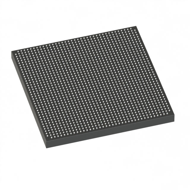
Stratix® V GX Field Programmable Gate Array (FPGA) IC 600 46080000 490000 1517-BBGA, FCBGA |
|---|---|
| Quantity | 77 Available (as of June 15, 2026) |

| Product Category | Field Programmable Gate Array (FPGA) |
|---|---|
| Manufacturer | Intel |
| Manufacturing Status | Active |
| Manufacturer Standard Lead Time | 26 Weeks |
| Datasheet |
Specifications & Environmental
| Device Package | 1517-FBGA (40x40) | Grade | Commercial | Operating Temperature | 0°C – 85°C | ||
|---|---|---|---|---|---|---|---|
| Package / Case | 1517-BBGA, FCBGA | Number of I/O | 600 | Voltage | 870 mV - 930 mV | ||
| Mounting Method | Surface Mount | RoHS Compliance | RoHS Compliant | REACH Compliance | REACH Unaffected | ||
| Moisture Sensitivity Level | 3 (168 Hours) | Number of LABs/CLBs | 185000 | Number of Logic Elements/Cells | 490000 | ||
| Number of Gates | N/A | ECCN | N/A | HTS Code | N/A | ||
| Qualification | N/A | Total RAM Bits | 46080000 |
Overview of 5SGXEA5N2F40C2G – Stratix® V GX FPGA, 600 I/Os, 490,000 logic elements
The 5SGXEA5N2F40C2G is a Stratix V GX Field Programmable Gate Array (FPGA) IC in a 1517-BBGA FCBGA package. It provides a high-density programmable logic platform with a large I/O complement and significant on-chip memory for commercial-grade embedded and system designs.
With approximately 490,000 logic elements, roughly 46 Mbits of embedded memory and up to 600 I/Os, this device is intended for designs that require extensive logic integration, wide external interfacing, and high routing density within a surface-mount FCBGA package.
Key Features
- Core Capacity Approximately 490,000 logic elements (logic cells) to implement large-scale digital designs and complex logic functions.
- Embedded Memory Total on-chip RAM of 46,080,000 bits (approximately 46 Mbits) to support buffering, lookup tables, and memory-intensive processing.
- I/O Resources Up to 600 I/Os to support extensive external connectivity and high-pin-count system interfaces.
- Package and Mounting 1517-BBGA (FCBGA) supplier device package 1517-FBGA (40×40) in a surface-mount form factor for high-density board integration.
- Power Supply Core supply range specified at 870 mV to 930 mV, enabling predictable core voltage planning in system power architectures.
- Temperature Grade Commercial grade operating range from 0 °C to 85 °C for standard commercial-environment deployments.
- Regulatory RoHS compliant, supporting lead-free assembly and regulatory requirements for commercial products.
Typical Applications
- High-density logic implementations Designs that require extensive programmable logic capacity and complex data-paths can leverage the device's approximately 490,000 logic elements.
- Memory-intensive processing Applications that need significant on-chip buffering or LUT storage can use the approximately 46 Mbits of embedded memory.
- High I/O system interfaces Systems requiring many external connections and flexible pinout options benefit from up to 600 available I/Os.
- Compact, high-pin-count boards Surface-mount FCBGA packaging (1517-BBGA) enables dense board layouts where area and pin count are critical.
Unique Advantages
- High logic density: The large logic-element count enables consolidation of multiple functions into a single FPGA, reducing component count.
- Substantial on-chip memory: Approximately 46 Mbits of embedded RAM supports larger buffers and state storage without external memory dependence.
- Extensive I/O capability: Up to 600 I/Os allow flexible interfacing to a wide range of peripherals, sensors, and high-speed front-ends.
- Commercial temperature and RoHS compliance: Specified 0 °C to 85 °C operation and RoHS status simplify qualification for commercial products and manufacturing processes.
- Standard surface-mount package: 1517-BBGA (40×40) FCBGA package supports compact PCB design and established assembly workflows.
- Defined core voltage window: 870 mV to 930 mV supply specification assists in predictable power-supply design and system integration.
Why Choose 5SGXEA5N2F40C2G?
The 5SGXEA5N2F40C2G delivers a balance of very high logic capacity, significant embedded memory, and a large I/O complement in a compact FCBGA package. Its commercial-grade operating range and RoHS compliance make it suitable for mainstream embedded, communications, and compute-centric designs that require dense integration and flexible external interfacing.
Engineers and procurement teams looking to consolidate multiple functions into a single programmable device will find this Stratix V GX FPGA well suited for projects that demand high logic density, ample on-chip RAM, and extensive I/O without changing package architecture or assembly flow.
Request a quote or submit a pricing inquiry for part number 5SGXEA5N2F40C2G to receive availability and ordering information tailored to your project requirements.


Date Founded: 1968
Headquarters: Santa Clara, California, USA
Employees: 130,000+
Revenue: $54.23 Billion
Certifications and Memberships: ISO9001:2015, ISO14001:2015, ISO17025:2017, ISO27001:2022, ISO45001:2018, ISO50001:2018


